|
Материал взят на персональной странице Jim Plusquellic , профессора Питтсбургского университета
-
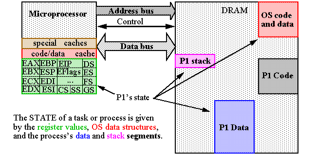
Что входит в понятие выполняемой программы (процесса или задачи)?
-
Если процесс
P2
создан и запущен (он здесь не показан), параметры процесса
P1
должны быть сохранены так , чтобы его можно было выполнять и дальше .
-
Поскольку каждый регистр существует в единственном экземпляре , его состояние должно быть сохранено в памяти.
-
Позже мы увидим , как это поддерживается на пентиуме.
-
Перейдем к организации и управлению памяти.
-
В идеале было бы недурно иметь бесконечно большую память.
-
Реально память состоит из:
-
Cache
(SRAMS): маленькая и очень быстрая.
-
Main Memory
(DRAM): большая и помедленнее.
-
Disk
: ну очень большая и совсем медленная.
-
OS обречена на управление этими ограниченными ресурсами и созданием иллюзии быстрой и бесконечной памяти.
-
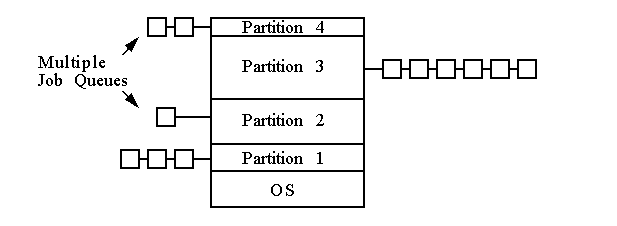
-
При многозадачности оно сводится к разбиению памяти на
n
фиксированные порции.
-
Эти порции определяются на старте системы и могут быть использованы для хранения кода , данных и стека .
-
Преимущество : простота реализации.
-
Но это плохая схема . К тому же она пожирает много времени на сам процесс обслуживания очереди.
-
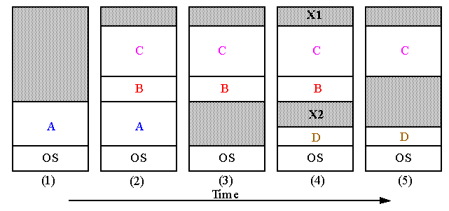
По этой схеме , число , расположение и размер выделяемой памяти для каждого процесса динамично меняются
-
(1) Вначале имеем один процесс
A
в памяти.
-
(2) Затем
B
и
C
.
-
(3)
A
выгружаем.
-
(4)
D
создаем,
B
выгружаем.
-
Этот метод улучшает использование памяти , но усложняет процесс ее выделения и освобождения тем ,
что создает дыры в памяти или фрагментирует ее
.
-
Можно конечно воспользоваться уплотнением памяти , но это сожрет ресурсы процессора .
-
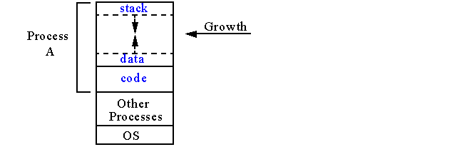
Размер данных может изменяться динамически например с помощью
malloc()
.
-
И если процессу некуда расти , его прийдется убить
.
-
hard disk может помочь в случае , если памяти не хватает.
-
Например , когда процесс блокируется клавиатурой , он может быть засвопирован
на диск и освобождая место другим процессам
.
-
Перемещение процесса на диск и обратно называется своппингом -
swapping
.
-
Диск может быть использован для реализации 2-й схемы - виртуальная память -
virtual memory
.
-
Виртуальная память позволяет процессам выполняться даже тогда , когда им не
хватает физической памяти
.
-
Это обычная практика для 32-битной архитектуры
.
-
Если OS поддерживает
virtual memory
, такие процессы могут быть представлены в памяти кусками -
порциями
.
-
При подкачке OS свопирует неиспользуемую
память
на диск.
-
Виртуальная память работет в мультизадачной системе
.
-
Основная память может хранить куски многих процессов.
-
Процесс стоит в очереди до тех пор , пока очередная порция не подкачена с диска
.
-
Своппинг сам по себе - также не очень эффективен
.
-
И тут опять виновата фрагментация
.
-
2 концепции:
-
Сегментация: Позволяет рационально использовать память
.
-
Пэйджинг: Эффективное управление физической памятью , реализация виртуальной памяти.
-
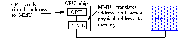
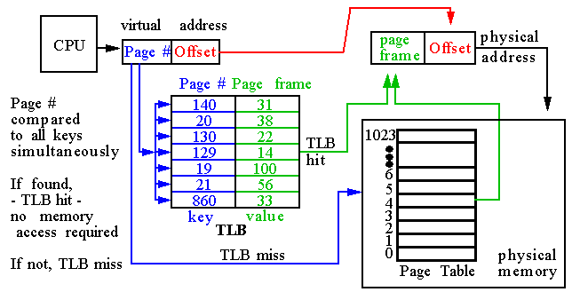
Адрес на адресной шине - это
физический адрес
.
-
Процесс генерит
виртуальный адрес
, например команда : MOV EAX, [EBX]
-
адрес памяти в [EBX] может вообще-то превышать размер доступной физической памяти.
-
Линейные адреса получаются из
виртуальных
с помощью сегментации
.
-
Виртуальный (или линейный) адрес трансформируется с помощью
Memory Management Unit
(MMU) в реальный физический адрес.
-
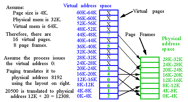
Виртуальное и физическое адресное пространство поделено на страницы
.
-
Размер такой страницы колеблется в пределах от 512 до 64000 байт и зависит от архитектуры .
-
Кроме страниц еще имеются фреймы
.
-
Размер страниц и фреймов одинаков.
-
Обратите внимание на то , что 8 виртуальных страниц не маппируются на физическую память (те , которые помечены
X
).
-
Пэйджинг разбивает адресное пространство процесса на несколько кусков
!
-
Тем самым мы решаем проблему фрагментации
.
-
Манипуляции с адресами в MMU
-
Page Table:
-
Размер
:
-
Пентиум использует 32-битные виртуальные адреса.
-
Если размер страницы 4K , с 32-битной адресацией имеем 2
32
/2
12
= 2
20
или 1,048,576 виртуальных страниц !
-
Если учесть что на адрес приходится 4 байта, получаем 4 метра памяти на всю page table.
-
Соответственно для 64-bit - 2
52
страниц !!!
-
Реализация
:
-
Перевод virtual-to-physical делается для
ВСЕХ
адресов.
-
Такой перевод должен быть максимально быстр.
-
Сама page table хранится в массиве.
-
OS загружает его при старте процесса.
-
При таком вызове page table обращение к ней идет напрямую без ссылок.
-
Недостаток в том , что при переключении процессов эту таблицу каждый раз нужно загружать заново.
-
Page table хранится в main memory.
-
ЕЕ адрес хранится в регистре .
-
При Context switches нужно лишь изменить значение этого регистра .
-
Последние версии чипов хранят "frequently used" адреса страниц в кеше
.
-
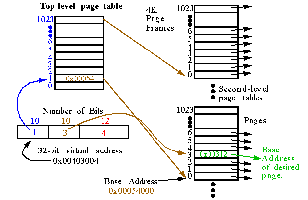
Имеется 2-уровневая модель.
-
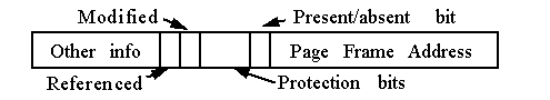
Page Frame address
: Most significant bits of physical memory address.
-
Present/Absent bit
: If 1, page is in memory, if 0, it is on disk.
-
Modified bit
: If set, page has been written to, e.g. it is `dirty'.
-
Referenced bit
: Used in the OS page replacement algorithm.
-
Protection bits
: Specifies if data in page can be read/written/executed.
-
With two-level paging, one memory reference could require three memory accesses !
-
In order to reduce the number of times this occurs, a fast lookup table called a
TLB
is added as a hardware cache in the microprocessor.
-
Number of TLB entries varies from 8 to 2048.
-
When a
TLB miss
occurs:
-
A trap occurs and an OS routine handles the fault. The instruction is then restarted.
-
The OS routine copies one (or more) page frame(s) from the page table in memory to one (or more) of the TLB entries.
-
Therefore, if page is referenced again soon, a
TLB hit
occurs eliminating the memory reference for the page frame.
-
Outline:
-
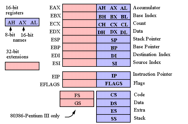
Internal
programmer visible
architecture, e.g. registers
-
Real Mode Addressing:
-
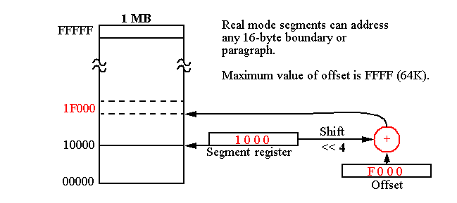
Real Mode Memory: 00000H-FFFFFH (the first 1MB of main memory).
-
Protected Mode Addressing:
-
All of memory (applicable to 80286 and later processors).
-
Programmer
in
visible
registers to control and operate the protected memory system.
-
Programmer visible registers:
-
General Purpose Registers: The main functions are listed.
-
EAX: Accumulator
: Referenced as EAX, AX, AL or AH.
-
Used for mult, div, etc.
-
Used to hold an offset.
-
EBX: Base Index
:
-
Used to hold the offset of a data pointer.
-
ECX: Count
:
-
Used to hold the count for some instructions, REP and LOOP.
-
Used to hold the offset of a data pointer.
-
EDX: Data
:
-
Used to hold a portion of the result for mult, of the operand for div.
-
Used to hold the offset of a data pointer.
-
EBP: Base Pointer
:
-
Holds the base pointer for memory data transfers.
-
EDI: Destination Index
:
-
Holds the base destination pointer for string instructions.
-
ESI: Source Index
:
-
Holds the base source pointer for string instructions.
-
Special Purpose Registers:
-
EIP: Instruction Pointer
:
-
Points to the next instruction in a code segment.
-
16-bits (IP) in real mode and 32-bits in protected mode.
-
ESP: Stack Pointer
:
-
Used by the stack, call and return instructions.
-
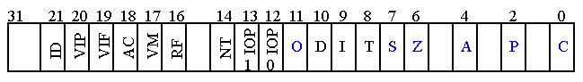
EFLAGS
:
-
Store the state of various conditions in the microprocessor.
-
Special Purpose Registers:
-
The rightmost 5 flag bits and overflow change after
many of the arithmetic and logic instructions execute. Data transfer
and control instructions never change the flags.
-
C (Carry)
:
-
Holds the carry out after addition or the borrow after subtraction.
-
Also indicates error conditions.
-
P (Parity)
:
-
0 for odd number of bits and 1 for even.
-
Obsolete feature of the 80x86.
-
A (Auxiliary Carry)
:
-
Highly specialized flag used by DAA and DAS instructions after BCD addition or subtraction.
-
Special Purpose Registers:
-
EFLAGS
(cont).
-
Z (Zero)
:
-
1 if the result of an arithmetic or logic instruction is 0.
-
S (Sign)
:
-
1 if the sign of the result of an arith. or logic instruction is negative.
-
T (Trap)
:
-
Trap enable. The microprocessor interrupts the flow of instructions on conditions indicated by the debug and control registers.
-
I (Interrupt)
:
-
Controls the operation of the INTR (Interrupt request) pin. If 1, interrupts are enabled. Set by
STI
and
CLI
instructions.
-
D (Direction)
:
-
Selects with increment or decrement mode for the DI and/or SI registers
during string instructions. If 1, registers are automatically
decremented. Set by
STD
and
CLD
instructions.
-
O (Overflow)
:
-
Set for addition and subtraction instructions.
-
Special Purpose Registers:
-
EFLAGS
(cont).
-
80286 and up:
-
IOPL (I/O privilege level)
:
-
It holds the privilege level at which your code must be running in
order to execute any I/O-related instructions. 00 is the highest.
-
NT (Nested Task)
:
-
Set when one system task has invoked another through a CALL instruction in protected mode.
-
80386 and up:
-
RF (Resume)
:
-
Used with debugging to selectively mask some exceptions.
-
VM (Virtual Mode)
:
-
When 0, the CPU can operate in Protected mode, 286 Emulation mode or
Real mode. When set, the CPU is converted to a high speed 8086. This
bit has enormous impact.
-
Special Purpose Registers:
-
EFLAGS
(cont).
-
80486SX and up:
-
AC (Alignment Check)
:
-
Specialized instruction for the 80486SX.
-
Pentium and up:
-
VIF (Virtual Interrupt Flag)
:
-
Copy of the interrupt flag bit.
-
VIP (Virtual Interrupt Pending)
:
-
Provides information about a virtual mode interrupt.
-
ID (Identification)
:
-
Supports the CPUID instruction, which provides version number and manufacturer information about the microprocessor.
-
Segment Registers:
-
CS (Code Segment)
:
-
In real mode, this specifies the start of a 64KB memory segment.
-
In protected mode, it selects a descriptor.
-
The code segment is limited to 64KB in the 8086-80286 and 4 GB in the 386 and above.
-
DS (Data Segment)
:
-
Similar to the CS except this segment holds data.
-
ES (Extra Segment)
:
-
Data segment used by some string instructions to hold destination data.
-
SS (Stack Segment)
:
-
Similar to the CS except this segment holds the stack.
-
ESP and EBP hold offsets into this segment.
-
FS and GS
: 80386 and up.
-
Allows two additional memory segments to be defined.
-
Only mode available to the 8086 and 8088.
-
Allow the processor to address only the first 1MB of memory.
-
DOS requires real mode.
-
Segments and Offsets
:
-
Effective address = Segment address + an offset.
-
Segments and Offsets
:
-
Syntax is usually given as
seg_addr:offset
, e.g.
1000:F000
in the previous example to specify
1F000H
.
-
Implicit combinations of segment registers and offsets are defined for memory references.
-
For example, the code segment (CS) is always used with the instruction pointer (IP for real mode or EIP for protected mode).
-
CS:EIP
-
SS:ESP
,
SS:EBP
-
DS:EAX
,
DS:EBX
,
DS:ECX
,
DS:EDX
,
DS:EDI
,
DS:ESI
,
DS:8-bit_literal
,
DS:32-bit_literal
-
ES:EDI
-
FS
and
GS
have no default.
-
It is illegal to place an offset larger than FFFF into the 80386 32-bit registers operating in Real Mode.
-
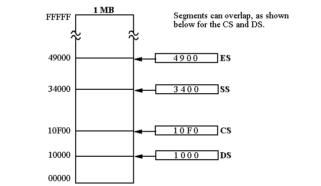
Segmented addressing allows relocation of data and code.
-
OS can assign the segment addresses at run time.
-
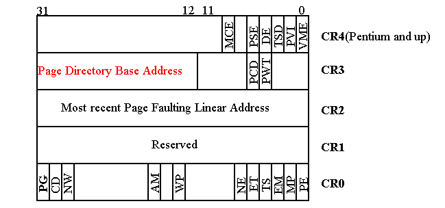
Memory Paging:
-
Available in the 80386 and up.
-
Allows a
linear address
(
virtual address
) of a program to be located in any portion of
physical
memory.
-
The
paging unit
is controlled by the microprocessors control registers:
-
Memory Paging:
-
The paging system operates in both real and protected mode.
-
It is enabled by setting the
PG
bit to 1 (left most bit in
CR0
).
-
(If set to 0, linear addresses are physical addresses).
-
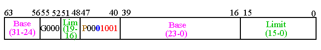
CR3
contains the
page directory
"physical" base address.
-
The value in this register is one of the few "physical" addresses you will ever refer to in a running system.
-
The
page directory
can reside at any 4K boundary since the low order 12 bits of the address are set to zero.
-
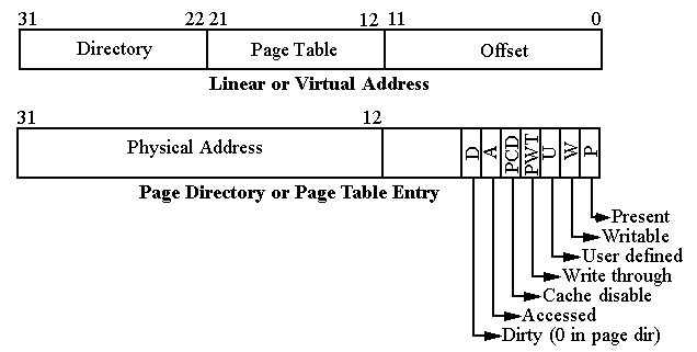
The
page directory
contains 1024 directory entries of 4 bytes each.
-
Each
page directory
entry addresses a
page table
that contains up to 1024 entries.
-
The virtual address is broken into three pieces:
-
Directory
: Each
page directory
addresses a 4MB section of main mem.
-
Page Table
: Each
page table
entry addresses a 4KB section of main mem.
-
Offset
: Specifies the byte in the page.
-
Memory Paging:
-
The
page directory
is 4K bytes.
-
Each
page table
is 4K bytes, and there are 1024 of them.
-
If all 4GB of memory is paged, the overhead is 4MB!
-
The current scheme requires three accesses to memory:
-
One to the
directory
, one to the appropriate
page table
and (finally) one to the desired data or code item. Ouch!
-
A
Translation Look-aside Buffer
(
TLB
) is used to cache page directory and page table entries to reduce the number of memory references.
-
Plus the data cache is used to hold recently accessed memory blocks.
-
System performance would be extremely bad without these features.
-
Much more on this in OS (CMSC 421).
-
Paging and Segmentation:
-
These two addresses translation mechanism are typically combined.
-
We'll look at this in later chapters.
-
-
The application programmer loads segment register values as before in
Real Mode, but the values that he/she puts in them are very different.
-
Since knowledge of the GDT and LDT is
not
generally available at compile time, the programmer must use symbolic names.
-
The
loader
is responsible for resolving the actual values at run time.
-
In general, the segment values are
16-bit tags
for the address spaces of the program.
-
Instructions such as
LDS
(load DS),
LAR
(load access rights),
LSL
(load segment limit),
VERR
(verify for read) are available to retrieve
descriptor
attributes, if the process is privileged enough.
-
Whenever a segment register is changed,
sanity checks
are performed before the descriptor is cached.
-
The index is checked against the limit.
-
Other checks are made depending on the segment
type, e.g., data segments, DS cannot be loaded with pointers to
execute-only descriptors, ...
-
The present flag is checked.
-
Otherwise, an exception is raised and nothing changes.
-
0: highest privilege, 3: lowest privilege
-
The privilege protection system plays a role for almost every instruction executed.
-
Protection mechanisms check if the process is privileged enough to:
-
Execute certain instructions
, e.g., those that modify the Interrupt flag, alter the segmentation, or affect the protection mechanism require PL 0.
-
Reference data other than its own
. References to data at
higher
privilege levels is not permitted.
-
Transfer control to code other than its own
. CALLs or JMPs to code with a
different
privilege level (higher or lower) is not permitted.
-
Privilege levels are
assigned to segments
, as we have seen, using the
DPL
(Descriptor Privilege Level) field (bits 45 and 46).
-
Define
CPL
as the
Code Privilege Level
of the process, which is the
DPL
of its
code segment
!
-
Define
RPL
as the Requestor's Privilege Level.
-
Privilege Level Definitions:
-
When data selectors are loaded, the corresponding data segment's DPL is compared to the
larger
of your CPL or the selector's RPL.
-
Therefore, you can use RPL to
weaken
your current privilege level, if you want.
-
CPL is defined by the descriptors, so access to them must be restricted.
-
Privileged Instructions:
-
Those that affect the segmentation and protection mechanisms (CPL=0 only).
-
For example, LGDT, LTR, HLT.
-
Those that alter the Interrupt flag (CPL <= IOPL field in EFLAGS).
-
For example, CLI, STI (Note: only DPL 0 code can modify the
IOPL
fields.)
-
Those that perform peripheral I/O (CPL <= IOPL field in EFLAGS).
-
Privileged Data References:
-
Two checks are made in this case:
-
Trying to load
the DS, ES, FS or GS register with a selector whose DPL is > the DPL of the code segment descriptor generates a
general protection fault
.
-
Trying to use
a data descriptor that has the proper privilege level can also be illegal, e.g. trying to write to a read-only segment.
-
For
SS
, the rules are even more restrictive.
-
Privileged Code References:
-
Transferring control to code in another segment is performed using the FAR forms of JMP, CALL and RET.
-
These differ from intra-segment (NEAR) transfers in that they change
both
CS and EIP.
-
The following checks are performed:
-
The new selector must be a code segment (e.g. with execute attribute).
-
CPL is set to the DPL (RPL is of no use here).
-
The segment is present.
-
The EIP is within the limits defined by the segment descriptor.
-
The RPL field is always set to the CPL of the process, independent of what was actually loaded.
-
You can examine the RPL field of CS to determine your CPL.
-
There are two ways to
change
your CPL:
-
Conforming Code segments
.
-
Remember Types 6 and 7 defined in the AR byte of descriptor?
-
Segments defined this way have no privilege level -- they conform to the level of the calling program.
-
This mechanism is well suited to handle programs that share code but run at different privilege levels, e.g., shared libraries.
-
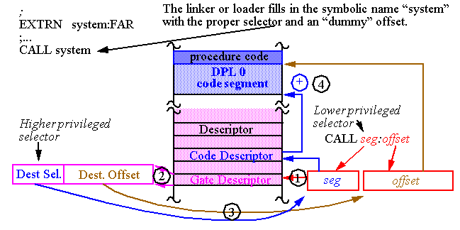
Through special segment descriptors called
Call Gates
.
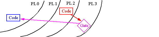
-
Call gates act as an interface layer between code segments at different privilege levels.
-
They define
entry points
in more privileged code to which control can be transferred.
-
They must be referred to using FAR CALL instructions (no JMPs are allowed).
-
Note, references to call gates are
indistinguishable
from other FALL CALLs in the program -- a segment and offset are still both given.
-
However, in this case, both are ignored and the call gate data is used instead.
-
Call Gate Mechanism:
-
Note that both the
selector
and
offset
are given in the call gate preventing lower privileged programs from jumping into the middle of higher privileged code.
-
This mechanism makes the higher privileged code
invisible
to the caller.
-
Call Gates have "tolls" as well, making some or all of them inaccessible to lower privileged processes.
-
The rule is that the Call Gate's DPL field (bits 45-46) MUST be >=
(lower in privilege) than the process's CPL before the call.
-
Moreover, the privileged code segment's DPL field MUST be <= the process's CPL before the call.
-
Changing privilege levels requires a
change in the stack
as well (otherwise, the protection mechanism would be sabotaged).
-
Stack segment DPLs MUST match the CPL of the process.
-
This happens transparently to the program code on both sides of the call gate!
-
Where does the new stack come from?
-
From yet another descriptor, Task State Segment (
TSS
) descriptor, and a special segment, the TSS.
-
The TSS stores the state of all tasks in the system and is described using a TSS descriptor.
-
The processor saves all the information it needs to know about a task in the TSS.
-
More on this later as time permits.
-
Two basic types:
-
ROM
: Read-only memory
-
RAM
: Read-Write memory
-
Four commonly used memories:
-
ROM
-
Flash (EEPROM)
-
Static RAM (SRAM)
-
Dynamic RAM (DRAM)
-
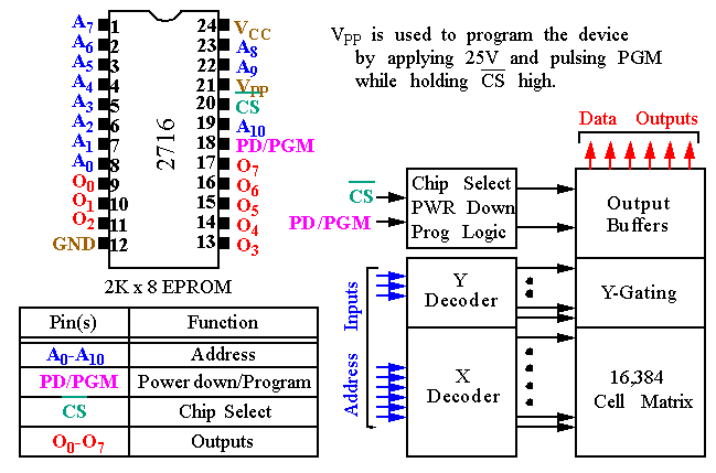
Generic pin configuration:
-
The number of address pins is related to the number of
memory locations
.
-
Common sizes today are
1K
to
256M
locations.
-
Therefore, between 10 and 28 address pins are present.
-
The data pins are typically
bi-directional
in read-write memories.
-
The number of data pins is related to the size of the
memory location
.
-
For example, an 8-bit wide (byte-wide) memory device has
8
data pins.
-
Catalog listing of
1K X 8
indicate a byte addressable
8K
memory.
-
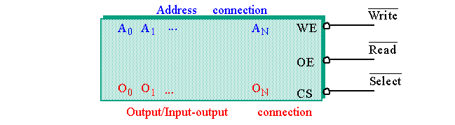
Each memory device has at least one
chip select
(
CS
) or
chip enable
(
CE
) or
select
(
S
) pin that enables the memory device.
-
This enables read and/or write operations.
-
If more than one are present, then all must be 0 in order to perform a read or write.
-
Each memory device has at least one control pin.
-
For ROMs, an
output enable
(
OE
) or
gate
(
G
) is present.
-
The
OE
pin enables and disables a set of tristate buffers.
-
For RAMs, a
read-write
(
R/W
) or
write enable
(
WE
) and
read enable
(OE
) are present.
-
For dual control pin devices, it must be hold true that both are not 0 at the same time.
-
ROM:
-
Non-volatile memory: Maintains its state when powered down.
-
There are several forms:
-
ROM
: Factory programmed, cannot be changed. Older style.
-
PROM
: Programmable Read-Only Memory.
-
Field programmable but only once. Older style.
-
EPROM
: Erasable Programmable Read-Only Memory.
-
Reprogramming requires up to 20 minutes of high-intensity UV light exposure.
-
ROMs (cont):
-
Flash EEPROM
: Electrically Erasable Programmable ROM.
-
Also called
EAROM
(Electrically Alterable ROM) and
NOVRAM
(NOn-Volatile RAM).
-
Writing is much slower than a normal RAM.
-
Used to store setup information, e.g. video card, on computer systems.
-
Can be used to replace EPROM for BIOS memory.
-
Intel 2716 EPROM (2K X 8):
-
Sample of the data sheet for the 2716 A.C. Characteristics.
|
Symbol
|
Parameter
|
Limits
|
Unit
|
Test Condition
|
|
Min
|
Typ.
|
Max
|
|
tACC1
|
Addr. to Output Delay
|
|
250
|
450
|
ns
|
PD/PGM= CS =VIL
|
|
tOH
|
Addr. to Output Hold
|
0
|
|
|
ns
|
PD/PGM= CS =VIL
|
|
tDF
|
Chip Deselect to Output Float
|
0
|
|
100
|
ns
|
PD/PGM=VIL
|
|
...
|
...
|
...
|
...
|
...
|
...
|
...
|
-
This EPROM requires a wait state for use with the 8086 (
460ns
constraint).
-
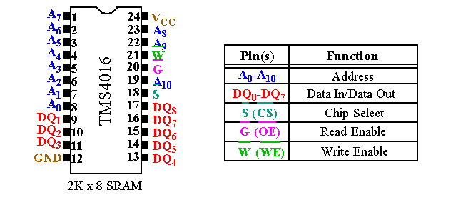
TI TMS 4016 SRAM (2K X 8):
-
Virtually identical to the EPROM with respect to the pinout.
-
However, access time is faster (250ns).
-
See the timing diagrams and data sheets in text.
-
SRAMs used for
caches
have access times as low as
10ns
.
-
DRAM:
-
SRAMs are limited in size (up to about 128K X 8).
-
DRAMs are available in much larger sizes, e.g., 64M X 1.
-
DRAMs MUST be refreshed (rewritten) every
2
to
4
ms
-
Since they store their value on an integrated capacitor that loses charge over time.
-
This refresh is performed by a special circuit in the DRAM which refreshes the entire memory using
256
reads.
-
Refresh also occurs on a normal read, write or during a special refresh cycle.
-
More on this later.
-
The large storage capacity of DRAMs make it impractical to add the required number of address pins.
-
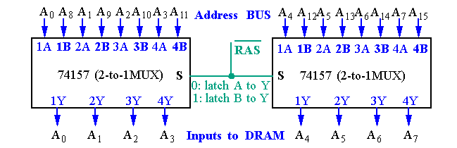
Instead, the address pins are
multiplexed
.
-
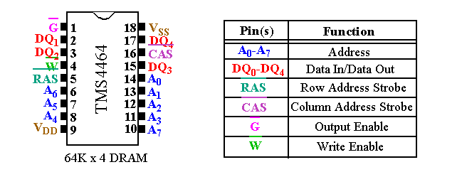
TI TMS4464 DRAM (64K X 4):
-
The TMS4464 can store a total of 256K bits of data.
-
It has
64K
addressable locations which means it needs
16
address inputs, but it has only
8
.
-
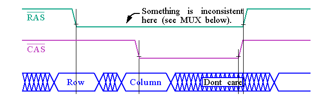
The row address (A
0
through A
7
) are placed on the address pins and strobed into a set of internal latches.
-
The column addres (A
8
through A
15
) is then strobed in using CAS.
-
TI TMS4464 DRAM (64K X 4) Timing Diagram:
-
CAS
also performs the function of the chip select input.
-
Larger DRAMs are available which are organized as
1M X 1
,
4M X 1
,
16M X 1
,
64M X 1
(with
256M X 1
available soon).
-
DRAMs are typically placed on SIMM (Single In-line Memory Modules) boards.
-
30-pin
SIMMs come in
1M X 8
,
1M X 9
(parity),
4M X 8
,
4M X 9
.
-
72-pin
SIMMs come in
1
/
2
/
3
/
8
/
16M X 32
or
1M X 36
(parity).
-
Pentiums have a 64-bit wide data bus.
-
The
30-pin
and
72-pin
SIMMs are not used on these systems.
-
Rather,
64-bit DIMMs
(
Dual In-line Memory Modules)
are the standard.
-
These organize the memory 64-bits wide.
-
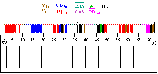
The board has DRAMs mounted on both sides and is
168
pins.
-
Sizes include
2M X 64
(
16M
),
4M X 64
(
32M
),
8M X 64
(
64M
) and
16M X 64
(
128M
).
-
The DIMM module is available in
DRAM
,
EDO
and
SDRAM
(and
NVRAM
) with and without an EPROM.
-
The EPROM provides information abou the size and speed of the memory device for PNP applications.
-
The processor can usually address a memory space that is
much larger
than the memory space covered by an individual memory chip.
-
In order to splice a memory device into the address space of the processor, decoding is necessary.
-
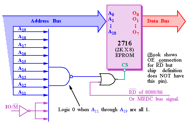
For example, the 8088 issues
20-bit
addresses for a total of
1MB
of memory address space.
-
However, the BIOS on a 2716 EPROM has only 2KB of memory and
11
address pins.
-
A decoder can be used to decode the additional
9
address pins and allow the EPROM to be placed in
any
2KB section of the 1MB address space.
-
To determine the address range that a device is mapped into:
-
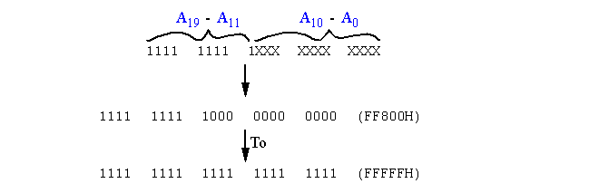
This 2KB memory segment maps into the
reset location
of the 8086/8088 (FFFF0H).
-
NAND gate decoders are not often used.
-
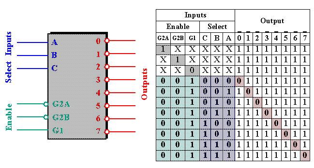
Rather the 3-to-8 Line Decoder (74LS138) is more common.
-
The 3-to-8 Line Decoder (74LS138)
-
Note that all
three
Enables (G2A, G2B, and G1) must be active, e.g. low, low and high, respectively.
-
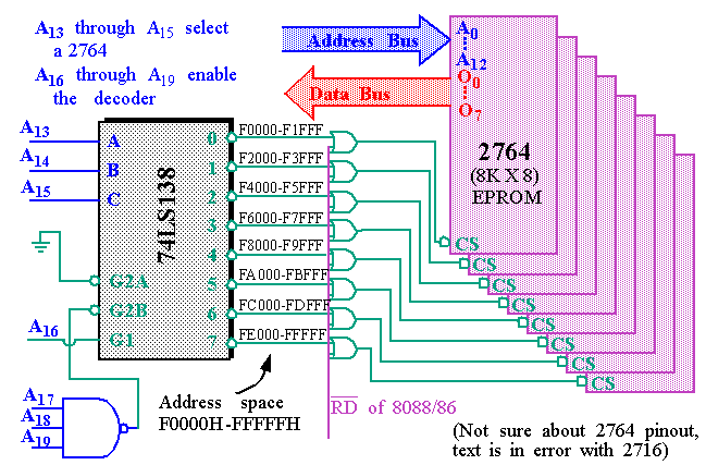
Each output of the decoder can be attached to an 2764 EPROM (
8K X 8
).
-
The EPROMs cover a 64KB section of memory.
-
Yet a third possibility is a
PLD
(Programmable Logic Device).
-
PLDs come in three varieties:
-
PLA
(Programmable Logic Array)
-
PAL
(Programmable Array Logic)
-
GAL
(Gated Array Logic)
-
PLDs have been around since the mid-1970s but have only recently
appeared in memory systems (PALs have replaced PROM address decoders).
-
PALs and PLAs are
fuse-programmed
(like the PROM).
-
Some are erasable (like the EPROM).
-
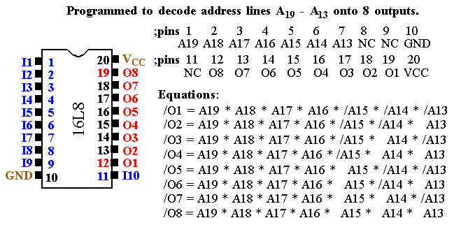
A PAL example (16L8) is shown in the text and is commonly used to
decode the memory address, particularly for 32-bit addresses generated
by the 80386DX and above.
-
AMD 16L8 PAL decoder.
-
It has 10 fixed inputs (Pins 1-9, 11), two fixed outputs (Pins 12 and 19) and 6 pins that can be either (Pins 13-18).
-
AND/NOR device with logic expressions (outputs) with up to 16 ANDed inputs and 7 ORed product terms.
-
The memory systems "sees" the 8088 as a device with:
-
20
address connections (A19 to A0).
-
8
data bus connections (AD7 to AD0).
-
3
control signals, IO/M, RD, and WR.
-
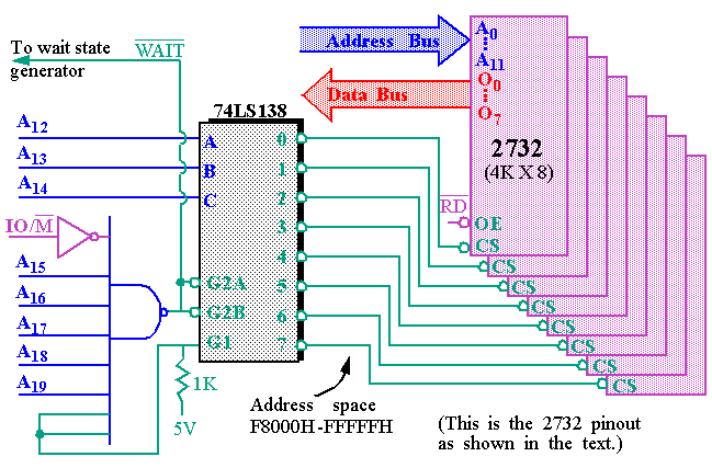
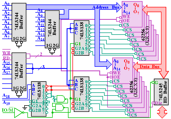
We'll look at interfacing the 8088 with:
-
32K
of EPROM (at addresses F8000H through FFFFFH).
-
512K
of SRAM (at addresses 00000H through 7FFFFH).
-
The EPROM interface uses a 74LS138 (3-to-8 line decoder) plus
8
2732 (
4K X 8
) EPROMs.
-
The EPROM will also require the generation of a wait state.
-
The EPROM has an access time of
450ns
.
-
The 74LS138 requires
12ns
to decode.
-
The 8088 runs at 5MHz and only allows
460ns
for memory to access data.
-
A wait state adds
200ns
of additional time.
-
The 8088 cold starts execution at
FFFF0H
. JMP to F8000H occurs here.
-
The
16
62256s on the previous slide are actually SRAMs.
-
Access times are on order of
10ns
.
-
Flash memory can also be interfaced to the 8088 (see text).
-
However, the write time (
400ms
!) is too slow to be used as RAM (as shown in the text).
-
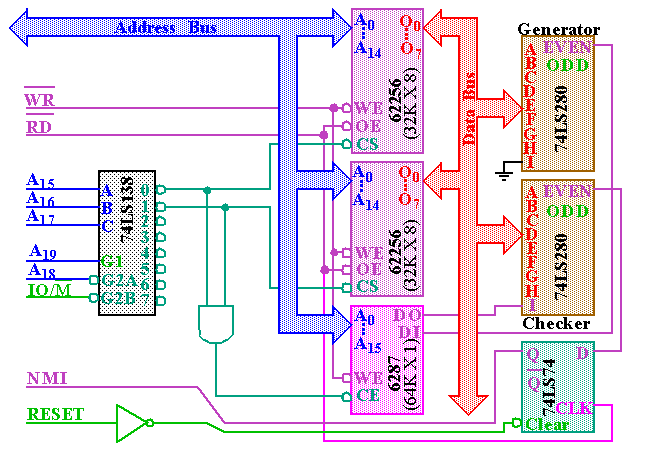
Parity Checking:
-
Parity checking is used to detect single bit errors in the memory.
-
The current trend is away from parity checking.
-
Parity checking adds
1
bit for every
8
data bits.
-
For
EVEN
parity, the
9th
bit is set to yield an even number of 1's in all 9 bits.
-
For
ODD
parity, the
9th
bit is set to make this number odd.
-
For 72-pin SIMMs, the number of data bits is 32 + 4 = 36 (
4
parity bits).
-
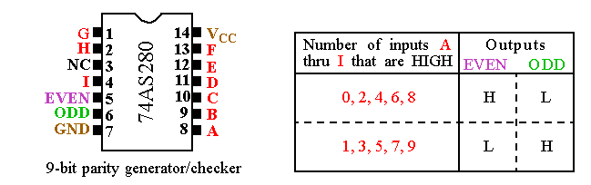
74AS280 Parity Generator/Checker
-
This circuit generates
EVEN
or
ODD
parity for the 9-bit number placed on its inputs.
-
Typically, for generation, the 9th input bit is set to 0.
-
This circuit also checks
EVEN
or
ODD
parity for the 9-bit number.
-
In this case, the
9th
input bit is connected to the
9th
bit of memory.
-
For example, if the original byte has an even # of 1's (with
9th
bit at GND), the parity bit is set to 1 (from the
EVEN
output).
-
If the
EVEN
output goes high during the check, then an error occurred.
-
This parity scheme can only detect a single bit error.
-
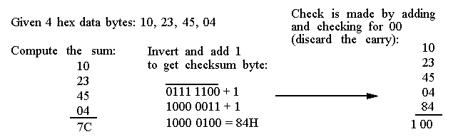
Block-Check Character (
BCC
) or Checksum.
-
Can detect
multiple bit
errors.
-
This is simply the
two's complement sum
(the negative of the sum) of the sequence of bytes.
-
No error occurred if adding the data values and the checksum produces a 0.
-
For example:
-
This is not fool proof.
-
If 45 changes to 44
AND
04 changes to 05, the error is missed.
-
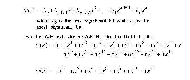
Cyclic Redundancy Check (
CRC
).
-
Commonly used to check data transfers in hardware such as harddrives.
-
Treats data as a stream of serial data
n-bits
long.
-
The bits are treated as coefficients of a
characteristic polynomial
,
M(X)
of the form:
-
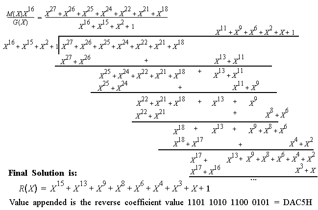
Cyclic Redundancy Check (
CRC
) (cont.)
-
The
CRC
is found by applying the following equation.
-
G(X)
is the called the
generator polynomial
and has special properties.
-
A commonly used polynomial is:
-
The remainder
R(X)
is
appended
to the data block.
-
When the
CRC
and
R(X)
is computed by the receiver,
R(X)
should be zero.
-
Since
G(X)
is of power 16, the remainder,
R(X)
, cannot be of order higher than 15.
-
Therefore, no more than
2
bytes are needed independent of the data block size.
-
Cyclic Redundancy Check (
CRC
)(cont.)
-
Parity
,
BCC
and
CRC
are only mechanisms for error detection.
-
The system is halted if an error is found in memory.
-
Error
correction
is starting to show up in new systems.
-
SDRAM
has ECC (Error Correction Code).
-
Correction will allow the system can continue operating.
-
If
two
errors occur, they can be
detected
but not
corrected
.
-
Error correction will of course cost more in terms of extra bits.
-
Error correction is based on
Hamming Codes
.
-
There is lots of theory here but our focus will be on implementation.
-
The objective is to correct any single bit errors in an 8-bit data byte.
-
In other words, we need
4
parity bits to correct single bit errors.
-
Note that the parity bits are at bit positions that are
powers of 2
.
-
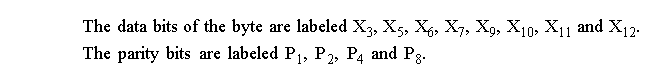
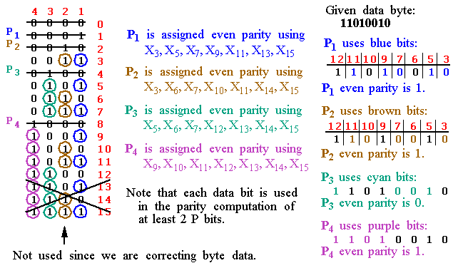
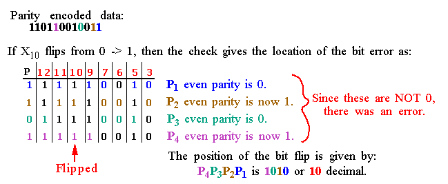
Hamming Codes (cont).
-
P1 is generated by computing the parity of X
3
, X
5
, X
7
, X
9
, X
11
, X
13
, X
15
.
-
These numbers have a 1 in bit position 1 of the subscript in binary.
-
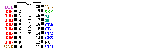
The 74LS636 corrects errors by storing
5
parity bits with each byte of data.
-
8
data I/O pins
-
5
check bit I/O pins
-
2
control pins
-
2
error outputs
-
Single error flag (
SEF
)
-
Double error flag (
DEF
).
-
See the text for an example of its use in a circuit.
|
| Evy | Очень полезная информация. Спасибо.
2009-05-12 21:38:53 | | Andrew | Ценный конспект. Но, увы, Intel назначил уровни привилегий по убывающей,
чтобы всех запутать. И здесь та же двусмысленность.
"Привилегии выше" -- это понятно. "Уровень привилегий выше" -- начинаются сомнения:
может, речь о том, что число больше (тогда это низшая привилегия).
2022-06-06 19:49:45 | |
|
|

 LINUX
LINUX 
 Languages