Что каждый программист должен знать о памяти , часть 1
Сентябрь 21, 2007
Автор - Ulrich Drepper
1 Введение
Раньше компьютеры были проще.
Процессоры , память , устройства хранения были единым целым.
Например , память и сетевые устройства были сопоставимы по скорости работы с процессором.
Но с какого-то момента разработчики начали оптимизировать отдельные компоненты.
В результате некоторые из них резко упали в производительности.
Это касается устройств хранения и памяти.
Операционные системы хранят основные данные в памяти,которая в свою очередь быстрее
остальных устройств хранения . У последних появился кеш , который прозрачен для операционных систем.
В отличие от устройств хранения , оптимизация памяти - намного более сложный процесс ,
который подчас идет на уровне железа.
Это имеет следующие формы:
- RAM hardware design (speed and parallelism).
- Memory controller designs.
- CPU caches.
- Direct memory access (DMA) for devices.
В этом документе будет идти речь о кеше процессора и DMA,
будут рассмотрены различные типы RAM.
1.1 Структура документа
Документ предназначен для широкой массы разработчиков ,
и не все подробные детали описания железа будут расшифрованы.
Вторая часть описывает т.н. random-access memory (RAM),
и ее полное понимание необязательно для остальных частей.
Вы можете найти тут полезные ссылки.
Третья часть описывает CPU cache.
Она является ключевой для понимания оставшегося документа.
4-я часть описывает реализацию виртуальной памяти и также важна.
5-я часть описывает т.н. Non Uniform Memory Access (NUMA).
6-я часть - центральная в этом документе.
В ней подводятся предварительные итоги и даются советы программистам , как лучше писать
в различных ситуациях.
В принципе , чтение документа можно начать прямо с нее и потом возвращаться
по мере необходимости.
7-я часть посвящена всяким тулзам
8-я дает обзор перспективным технологиям будущего.
2 Commodity Hardware Today
Understanding commodity hardware is important because specialized
hardware is in retreat. Scaling these days is most often achieved
horizontally instead of vertically, meaning today it is more cost-effective
to use many smaller, connected commodity computers
instead of a few really large and exceptionally fast (and expensive)
systems. This is the case because fast and inexpensive network
hardware is widely available. There are still situations where the
large specialized systems have their place and these systems still
provide a business opportunity, but the overall market is dwarfed by
the commodity hardware market. Red Hat, as of 2007, expects that for
future products, the “standard building blocks” for most data
centers will be a computer with up to four sockets, each filled with a
quad core CPU that, in the case of Intel CPUs, will be
hyper-threaded. {Hyper-threading enables a single processor
core to be used for two or more concurrent executions with just a
little extra hardware.} This means the standard system in the data
center will have up to 64 virtual processors. Bigger machines will be
supported, but the quad socket, quad CPU core case is currently
thought to be the sweet spot and most optimizations are targeted for
such machines.
Large differences exist in the structure of commodity computers. That
said, we will cover more than 90% of such hardware by concentrating
on the most important differences. Note that these technical details
tend to change rapidly, so the the reader is advised to take the date
of this writing into account.
Over the years the personal computers and smaller servers standardized
on a chipset with two parts: the Northbridge and Southbridge.
Figure 2.1 shows this structure.
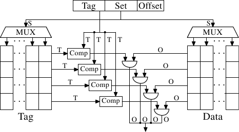
Figure 2.1: Structure with Northbridge and Southbridge
All CPUs (two in the previous example, but there can be more) are
connected via a common bus (the Front Side Bus, FSB) to the
Northbridge. The Northbridge contains, among other things, the memory
controller, and its implementation determines the type of RAM chips
used for the computer. Different types of RAM, such as DRAM, Rambus,
and SDRAM, require different memory controllers.
To reach all other system devices, the Northbridge must communicate with
the Southbridge. The Southbridge, often referred to as the I/O
bridge, handles communication with devices through a variety of
different buses. Today the PCI, PCI Express, SATA, and USB buses are
of most importance, but PATA, IEEE 1394, serial, and parallel ports
are also supported by the Southbridge. Older systems had AGP slots
which were attached to the Northbridge. This was done for performance
reasons related to insufficiently fast connections between the
Northbridge and Southbridge. However, today the PCI-E slots are all
connected to the Southbridge.
Such a system structure has a number of noteworthy consequences:
- All data communication from one CPU to another must travel over
the same bus used to communicate with the Northbridge.
- All communication with RAM must pass through the Northbridge.
- The RAM has only a single port.
{We will not discuss multi-port RAM in this document as this
type of RAM is not found in commodity hardware, at least not in places
where the programmer has access to it. It can be found in specialized
hardware such as network routers which depend on utmost speed.}
- Communication between a CPU and a device attached to the
Southbridge is routed through the Northbridge.
A couple of bottlenecks are immediately apparent in this design. One
such bottleneck involves access to RAM for devices. In the earliest
days of the PC, all communication with devices on either bridge had to
pass through the CPU, negatively impacting overall system performance.
To work around this problem some devices became capable of direct
memory access (DMA). DMA allows devices, with the help of the
Northbridge, to store and receive data in RAM directly without the
intervention of the CPU (and its inherent performance cost). Today all
high-performance devices attached to any of the buses can utilize DMA.
While this greatly reduces the workload on the CPU, it also creates
contention for the bandwidth of the Northbridge as DMA requests
compete with RAM access from the CPUs. This problem, therefore, must
to be taken into account.
A second bottleneck involves the bus from the Northbridge to the RAM.
The exact details of the bus depend on the memory types deployed.
On older systems there is only one bus to all the RAM chips, so
parallel access is not possible. Recent RAM types require
two separate buses (or channels as they are called for DDR2,
see Figure 2.8) which doubles the available bandwidth. The
Northbridge interleaves memory access across the channels. More
recent memory technologies (FB-DRAM, for instance) add more channels.
With limited bandwidth available, it is important to schedule memory
access in ways that minimize delays. As we will see, processors are much faster and
must wait to access memory, despite the use of CPU caches. If multiple
hyper-threads, cores, or processors access memory at the same time,
the wait times for memory access are even longer. This is also true
for DMA operations.
There is more to accessing memory than
concurrency, however. Access patterns themselves also greatly
influence the performance of the memory subsystem, especially with
multiple memory channels. Refer to Section 2.2 for more
details of RAM access patterns.
On some more expensive systems, the Northbridge does not actually
contain the memory controller. Instead the Northbridge can be
connected to a number of external memory controllers (in the following
example, four of them).
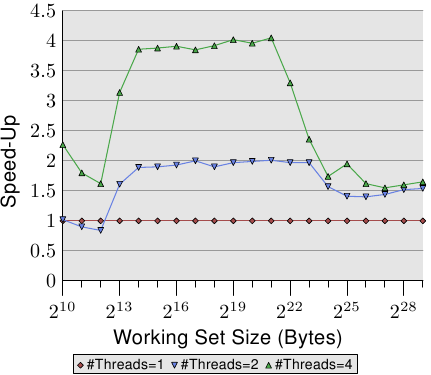
Figure 2.2: Northbridge with External Controllers
The advantage of this architecture is that more than one memory bus
exists and therefore total bandwidth increases. This design also
supports more memory. Concurrent memory access patterns reduce delays
by simultaneously accessing different memory banks. This is
especially true when multiple processors are directly connected to
the Northbridge, as in Figure 2.2. For such a design, the
primary limitation is the internal bandwidth of the Northbridge, which
is phenomenal for this architecture (from Intel). {For
completeness it should be mentioned that such a memory controller
arrangement can be used for other purposes such as “memory RAID”
which is useful in combination with hotplug memory.}
Using multiple external memory controllers is not the only way to
increase memory bandwidth. One other increasingly popular way is to integrate
memory controllers into the CPUs and attach memory to each CPU. This
architecture is made popular by SMP systems based on AMD's Opteron
processor. Figure 2.3 shows such a system. Intel will have
support for the Common System Interface (CSI) starting with the
Nehalem processors; this is basically the same approach: an integrated
memory controller with the possibility of local memory for each
processor.
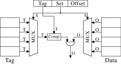
Figure 2.3: Integrated Memory Controller
With an architecture like this there are as many memory banks
available as there are processors. On a quad-CPU machine the memory
bandwidth is quadrupled without the need for a complicated Northbridge with
enormous bandwidth. Having a memory controller integrated into the
CPU has some additional advantages; we will not dig deeper into this
technology here.
There are disadvantages to this architecture, too. First of all,
because the machine still has to make all the memory of the system
accessible to all processors, the memory is not uniform anymore (hence
the name NUMA - Non-Uniform Memory Architecture - for such an architecture).
Local memory (memory attached to a processor)
can be accessed with the usual speed. The situation is different when
memory attached to another processor is accessed. In this case
the interconnects between the processors have to be used. To access
memory attached to CPU2 from CPU1 requires communication across one
interconnect. When the same CPU accesses memory attached to
CPU4 two interconnects have to be crossed.
Each such communication has an associated cost. We talk about “NUMA
factors” when we describe the extra time needed to access remote
memory. The example architecture in Figure 2.3 has two
levels for each CPU: immediately adjacent CPUs and one CPU
which is two interconnects away. With more
complicated machines the number of levels can grow significantly. There are
also machine architectures (for instance IBM's x445 and SGI's
Altix series) where there is more than one type of connection. CPUs
are organized into nodes; within a node the time to access the
memory might be uniform or have only small NUMA factors. The
connection between nodes can be very expensive, though, and the NUMA
factor can be quite high.
Commodity NUMA machines exist today and will likely play an even greater
role in the future. It is expected that, from late 2008 on, every SMP
machine will use NUMA. The costs associated with NUMA make it important to
recognize when a program is running on a NUMA machine. In
Section 5 we will discuss more machine architectures and some
technologies the Linux kernel provides for these programs.
Beyond the technical details described in the remainder of this
section, there are several additional factors which influence the
performance of RAM. They are not controllable by software, which is
why they are not covered in this section. The interested reader can
learn about some of these factors in Section 2.1. They are really
only needed to get a more complete picture of RAM technology and
possibly to make better decisions when purchasing computers.
The following two sections discuss hardware details at the gate level
and the access protocol between the memory controller and the DRAM
chips. Programmers will likely find this information enlightening since these
details explain why RAM access works the way it does. It is optional
knowledge, though, and the reader anxious to get to topics with more
immediate relevance for everyday life can jump ahead to
Section 2.2.5.
2.1 RAM Types
There have been many types of RAM over the years and each type
varies, sometimes significantly, from the other. The older types are
today really only interesting to the historians. We will not explore
the details of those. Instead we will concentrate on modern RAM types;
we will only scrape the surface, exploring some details which are
visible to the kernel or application developer through their
performance characteristics.
The first interesting details are centered around the question why
there are different types of RAM in the same machine. More
specifically, why there are both static RAM (SRAM {In other contexts
SRAM might mean “synchronous RAM”.}) and dynamic RAM (DRAM). The
former is much faster and provides the same functionality. Why is not
all RAM in a machine SRAM? The answer is, as one might expect, cost.
SRAM is much more expensive to produce and to use than DRAM. Both
these cost factors are important, the second one increasing in
importance more and more. To understand these difference we look at
the implementation of a bit of storage for both SRAM and DRAM.
In the remainder of this section we will discuss some low-level
details of the implementation of RAM. We will keep the level of detail as
low as possible. To that end, we will discuss the signals at a “logic level” and not at
a level a hardware designer would have to use. That level of detail
is unnecessary for our purpose here.
2.1.1 Static RAM
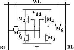
Figure 2.4: 6-T Static RAM
Figure 2.4 shows the structure of a 6 transistor SRAM cell.
The core of this cell is formed by the four transistors M1
to M4 which form two cross-coupled inverters. They have
two stable states, representing 0 and 1 respectively. The state is
stable as long as power on Vdd is available.
If access to the state of the cell is needed the word access line
WL is raised. This makes the state of the cell immediately
available for reading on BL and
BL. If the cell state must be
overwritten the BL and BL
lines are first set to the desired values and then WL is
raised. Since the outside drivers are stronger than the four
transistors (M1 through M4) this
allows the old state to be overwritten.
See [sramwiki] for a more detailed on the way the cell works.
For the following discussion it is important to note that
- one cell requires six transistors. There are variants with four
transistors but they have disadvantages.
- maintaining the state of the cell requires constant power.
- the cell state is available for reading almost immediately once
the word access line WL is raised. The signal is as rectangular
(changing quickly between the two binary states) as
other transistor-controlled signals.
- the cell state is stable, no refresh cycles are needed.
There are other slow and less power-hungry SRAM forms available, but
those are not of interest here since we are looking at fast RAM.
These slow variants are mainly interesting because they can be more
easily be used in a system than a dynamic RAM chip because of their
simpler interface.
2.1.2 Dynamic RAM
Dynamic RAM is, in its structure, much simpler than static RAM.
Figure 2.5 shows the structure of a usual DRAM cell design.
All it consists of is one transistor and one capacitor. This huge
difference in complexity of course means that it functions very differently
than static RAM.
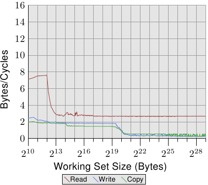
Figure 2.5: 1-T Dynamic RAM
A dynamic RAM cell keeps its state in the capacitor C. The
transistor M is used to guard the access to the state. To
read the state of the cell the access line AL is raised;
this either causes a current to flow on the data line DL or
not, depending on the charge in the capacitor. To write to the cell the
data line DL is appropriately
set and then AL is raised for a time long enough to charge or
drain the capacitor.
There are a number of complications with the design of dynamic RAM.
The use of a capacitor means that reading the cell discharges the
capacitor. The procedure cannot be repeated indefinitely, the
capacitor must be recharged at some point. Even worse, to accommodate
the huge number of cells (chips with 109 or more cells are now
common) the capacity to the capacitor must be low (in the femto-farad range
or lower). A fully charged capacitor holds a few 10's of thousands of
electrons. Even though the resistance of the capacitor is high (a
couple of tera-ohms) it only takes a short time for the capacity to
dissipate. This problem is called “leakage”.
This leakage is why a DRAM cell must be constantly refreshed. For most DRAM
chips these days this refresh must happen every 64ms. During the refresh cycle no access to
the memory is possible. For some workloads this overhead might stall
up to 50% of the memory accesses (see [highperfdram]).
A second problem resulting from the tiny charge is that the
information read from the cell is not directly usable. The data line
must be connected to a sense amplifier which can distinguish between
a stored 0 or 1 over the whole range of charges which still have to
count as 1.
A third problem is that charging and draining a capacitor is not
instantaneous. The signals received by the sense amplifier are not
rectangular, so a conservative estimate as to when the output of the
cell is usable has to be used. The formulas for charging and
discharging a capacitor are
![[Formulas]](images/capcharge.png)
This means it takes some time (determined by the capacity C and
resistance R) for the capacitor to be charged and discharged. It also
means that the current which can be detected by the sense amplifiers
is not immediately available. Figure 2.6 shows the charge and
discharge curves. The X—axis is measured in units of RC (resistance
multiplied by capacitance) which is a unit of time.
Figure 2.6: Capacitor Charge and Discharge Timing
Unlike the static RAM case where the output is immediately available when
the word access line is raised, it will always take a bit of time until the
capacitor discharges sufficiently. This delay severely limits how fast
DRAM can be.
The simple approach has its advantages, too. The main advantage is
size. The chip real estate needed for one DRAM cell is many times
smaller than that of an SRAM cell. The SRAM cells also need
individual power for the transistors maintaining the state. The
structure of the DRAM cell is also simpler and more regular which
means packing many of them close together on a die is simpler.
Overall, the (quite dramatic) difference in cost wins. Except in
specialized hardware — network routers, for example — we have to live with main memory
which is based on DRAM. This has huge implications on the programmer
which we will discuss in the remainder of this paper. But first we need
to look into a few more details of the actual use of DRAM cells.
2.1.3 DRAM Access
A program selects a memory location using a virtual address. The
processor translates this into a physical address and finally the
memory controller selects the RAM chip corresponding to that address. To
select the individual memory cell on the RAM chip, parts of the
physical address are passed on in the form of a number of address
lines.
It would be completely impractical to address memory locations
individually from the memory controller: 4GB of RAM would require
232 address lines.
Instead the address is passed encoded as a binary number using a
smaller set of address lines. The address passed to the DRAM chip
this way must be demultiplexed first. A demultiplexer with N
address lines will have 2N output lines. These output lines can be
used to select the memory cell. Using this direct approach is no big
problem for chips with small capacities.
But if the number of cells grows this approach is not suitable
anymore. A chip with 1Gbit
{I hate those SI prefixes. For me
a giga-bit will always be 230 and not 109 bits.}
capacity
would need 30 address lines and 230 select lines. The size of a
demultiplexer increases exponentially with the number of input lines
when speed is not to be sacrificed. A demultiplexer for 30 address
lines needs a whole lot of chip real estate in addition to the
complexity (size and time) of the demultiplexer. Even more
importantly, transmitting 30 impulses on the address lines
synchronously is much harder than transmitting “only” 15 impulses.
Fewer lines have to be laid out at exactly the same length or timed
appropriately. {Modern DRAM types like DDR3 can automatically
adjust the timing but there is a limit as to what can be tolerated.}
Figure 2.7: Dynamic RAM Schematic
Figure 2.7 shows a DRAM chip at a very high level. The DRAM
cells are organized in rows and columns. They could all be aligned in
one row but then the DRAM chip would need a huge demultiplexer. With
the array approach the design can get by with one demultiplexer and
one multiplexer of half the size. {Multiplexers and
demultiplexers are equivalent and the multiplexer here needs to work
as a demultiplexer when writing. So we will drop the differentiation
from now on.} This is a huge saving on all fronts. In the example
the address lines
a0 and
a1 through the row address
selection
(RAS)
demultiplexer select the address lines of a whole row of cells. When
reading, the content of all cells is thusly made available to the
column address selection
(CAS)
{The line over the name
indicates that the signal is negated} multiplexer. Based on the
address lines a2 and
a3 the content of one column is
then made available to the data pin of the DRAM chip. This happens
many times in parallel on a number of DRAM chips to produce a total
number of bits corresponding to the width of the data bus.
For writing, the new cell value is put on the data bus and, when the
cell is selected using the RAS and CAS, it is stored in the cell.
A pretty straightforward design. There are in reality — obviously — many
more complications. There need to be specifications how much delay there
is after the signal before the data will be available on the data bus for
reading. The capacitors do not unload instantaneously, as described
in the previous section. The signal from the cells is so weak that
it needs to be amplified. For writing it must be specified how long
the data must be available on the bus after the RAS and CAS is
done to successfully store the new value in the cell (again, capacitor
do not fill or drain instantaneously). These timing constants are
crucial for the performance of the DRAM chip. We will talk about this
in the next section.
A secondary scalability problem is that having 30 address lines
connected to every RAM chip is not feasible either. Pins of a chip
are a precious resources. It is “bad” enough that the data must be
transferred as much as possible in parallel (e.g., in 64 bit batches).
The memory controller must be able to address each RAM module
(collection of RAM chips). If parallel access to multiple RAM modules
is required for performance reasons and each RAM module requires its own
set of 30 or more address lines, then the memory controller needs to
have, for 8 RAM modules, a whopping 240+ pins only for the address
handling.
To counter these secondary scalability problems DRAM chips have, for a long
time, multiplexed the address itself. That means the address is
transferred in two parts. The first part consisting of address bits
a0 and
a1 in the example in
Figure 2.7) select the row. This selection remains active
until revoked. Then the second part, address bits
a2 and
a3, select the column. The
crucial difference is that only two external address lines are needed.
A few more lines are needed to indicate when the RAS and CAS signals
are available but this is a small price to pay for cutting the number
of address lines in half. This address multiplexing brings its own
set of problems, though. We will discuss them in Section 2.2.
2.1.4 Conclusions
Do not worry if the details in this section are a bit overwhelming.
The important things to take away from this section are:
- there are reasons why not all memory is SRAM
- memory cells need to be individually selected to be used
- the number of address lines is directly responsible for the cost
of the memory controller, motherboards, DRAM module, and DRAM chip
- it takes a while before the results of the read or write
operation are available
The following section will go into more details about the actual
process of accessing DRAM memory. We are not going into more details
of accessing SRAM, which is usually directly addressed. This happens
for speed and because the SRAM memory is limited in size. SRAM is
currently used in CPU caches and on-die where the connections are small
and fully under control of the CPU designer. CPU caches are a topic
which we discuss later but all we need to know is that SRAM cells have
a certain maximum speed which depends on the effort spent on the
SRAM. The speed can vary from only slightly slower than the CPU core
to one or two orders of magnitude slower.
2.2 DRAM Access Technical Details
In the section introducing DRAM we saw that DRAM chips multiplex the
addresses in order to save resources. We also saw that accessing DRAM
cells takes time since the capacitors in those cells do not discharge instantaneously
to produce a stable signal; we also saw that DRAM cells must be
refreshed. Now it is time to put this all together and see how all
these factors determine how the DRAM access has to happen.
We will concentrate on current technology; we will not discuss
asynchronous DRAM and its variants as they are simply not relevant
anymore. Readers interested in this topic are referred to
[highperfdram] and [arstechtwo]. We will also not talk about
Rambus DRAM (RDRAM) even though
the technology is not obsolete. It is just not widely used for system
memory. We will concentrate exclusively
on Synchronous DRAM (SDRAM) and its successors Double Data Rate DRAM
(DDR).
Synchronous DRAM, as the name suggests, works relative to a time
source. The memory controller provides a clock, the frequency of
which determines the speed of the Front Side Bus (FSB) —
the memory controller interface used by the DRAM chips. As of this writing,
frequencies of 800MHz, 1,066MHz, or even 1,333MHz are available with
higher frequencies (1,600MHz) being announced for the next generation. This
does not mean the frequency used on the bus is actually this high.
Instead, today's buses are double- or quad-pumped, meaning that data is
transported two or four times per cycle. Higher numbers sell so the
manufacturers like to advertise a quad-pumped 200MHz bus as an
“effective” 800MHz bus.
For SDRAM today each data transfer consists of 64 bits — 8 bytes. The
transfer rate of the FSB is therefore 8 bytes multiplied by the effective
bus frequency (6.4GB/s for the quad-pumped 200MHz bus). That sounds a
lot but it is the burst speed, the maximum speed which will never be
surpassed. As we will see now the protocol for talking
to the RAM modules has a lot of downtime when no data can be transmitted.
It is exactly this downtime which we must understand and minimize to
achieve the best performance.
2.2.1 Read Access Protocol
Figure 2.8: SDRAM Read Access Timing
Figure 2.8 shows the activity on some of the connectors of
a DRAM module which happens in three differently colored phases. As
usual, time flows from left to right. A lot of details are left out.
Here we only talk about the bus clock, RAS and CAS signals, and
the address and data buses. A read cycle begins with the memory
controller making the row address available on the address bus and
lowering the RAS signal. All signals are read on the rising edge
of the clock (CLK) so it does not matter if the signal is not
completely square as long as it is stable at the time it is read.
Setting the row address causes the RAM chip to start latching the
addressed row.
The CAS signal can be sent after tRCD (RAS-to-CAS Delay)
clock cycles. The column address is then transmitted by making it
available on the address bus and lowering the CAS line. Here we
can see how the two parts of the address (more or less halves, nothing
else makes sense) can be transmitted over the same address bus.
Now the addressing is complete and the data can be transmitted. The
RAM chip needs some time to prepare for this. The delay is usually
called CAS Latency (CL). In Figure 2.8 the CAS
latency is 2. It can be higher or lower, depending on the quality of
the memory controller, motherboard, and DRAM module. The latency can
also have half values. With CL=2.5 the first data would be available
at the first falling flank in the blue area.
With all this preparation to get to the data it would be wasteful to
only transfer one data word. This is why DRAM modules allow the
memory controller to specify how much data is to be transmitted.
Often the choice is between 2, 4, or 8 words. This allows filling
entire lines in the caches without a new RAS/CAS sequence. It is also
possible for the memory controller to send a new CAS signal without
resetting the row selection. In this way, consecutive memory addresses
can be read from or written to significantly faster because
the RAS signal does not have to be sent and the row does
not have to be deactivated (see below). Keeping the row “open” is
something the memory controller has to decide. Speculatively leaving
it open all the time has disadvantages with real-world applications
(see [highperfdram]). Sending new CAS signals is only subject
to the Command Rate of the RAM module (usually specified as Tx,
where x is a value like 1 or 2; it will be 1 for high-performance DRAM
modules which accept new commands every cycle).
In this example the SDRAM spits out one word per cycle. This is what
the first generation does. DDR is able to transmit two words per
cycle. This cuts down on the transfer time but does not change the
latency. In principle, DDR2 works the same although in practice it
looks different. There is no need to go into the details here. It is
sufficient to note that DDR2 can be made faster, cheaper, more
reliable, and is more energy efficient (see [ddrtwo] for more
information).
2.2.2 Precharge and Activation
Figure 2.8 does not cover the whole cycle. It only shows
parts of the full cycle of accessing DRAM. Before a new RAS signal
can be sent the currently latched row must be deactivated and the new
row must be precharged. We can concentrate here on the case where
this is done with an explicit command. There are improvements to the
protocol which, in some situations, allows this extra step to be avoided. The
delays introduced by precharging still affect the operation, though.
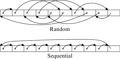
Figure 2.9: SDRAM Precharge and Activation
Figure 2.9 shows the activity starting from one CAS
signal to the CAS signal for another row. The data requested with
the first CAS signal is available as before, after CL cycles. In the
example two words are requested which, on a simple SDRAM, takes two
cycles to transmit. Alternatively, imagine four words on a DDR chip.
Even on DRAM modules with a command rate of one the precharge command
cannot be issued right away. It is necessary to wait as long as it
takes to transmit the data. In this case it takes two cycles. This
happens to be the same as CL but that is just a coincidence. The
precharge signal has no dedicated line; instead, some implementations
issue it by
lowering the Write Enable (WE) and RAS line simultaneously. This
combination has no useful meaning by itself (see [micronddr] for
encoding details).
Once the precharge command is issued it takes tRP (Row Precharge
time) cycles until the row can be selected. In Figure 2.9
much of the time (indicated by the purplish color) overlaps with the
memory transfer (light blue). This is good! But tRP is larger than
the transfer time and so the next RAS signal is stalled for one
cycle.
If we were to continue the timeline in the diagram we would find that
the next data transfer happens 5 cycles after the previous one stops.
This means the data bus is only in use two cycles out of seven.
Multiply this with the FSB speed and the theoretical 6.4GB/s for a
800MHz bus become 1.8GB/s. That is bad and must be avoided. The
techniques described in Section 6 help to raise this number.
But the programmer usually has to do her share.
There is one more timing value for a SDRAM module which we have not
discussed. In Figure 2.9 the precharge command was only
limited by the data transfer time. Another constraint is that an
SDRAM module needs time after a RAS signal before it can precharge
another row (denoted as tRAS). This number is usually pretty high,
in the order of two or three times the tRP value. This is a
problem if, after a RAS signal, only one CAS signal follows
and the data transfer is finished in a few cycles. Assume that in
Figure 2.9 the initial CAS signal was preceded directly
by a RAS signal and that tRAS is 8 cycles. Then the precharge
command would have to be delayed by one additional cycle since the sum of
tRCD, CL, and tRP (since it is larger than the data transfer time)
is only 7 cycles.
DDR modules are often described using a special notation: w-x-y-z-T.
For instance: 2-3-2-8-T1. This means:
| w | 2 | CAS Latency (CL) |
| x | 3 | RAS-to-CAS delay (tRCD) |
| y | 2 | RAS
Precharge (tRP) |
| z | 8 | Active to Precharge delay (tRAS) |
| T | T1 | Command Rate |
There are numerous other timing constants which affect the way
commands can be issued and are handled. Those five constants are in
practice sufficient to determine the performance of the module, though.
It is sometimes useful to know this information for the computers in
use to be able to interpret certain measurements. It is
definitely useful to know these details when buying computers since
they, along with the FSB and SDRAM module speed, are
among the most important factors determining a computer's speed.
The very adventurous reader could also try to tweak a system.
Sometimes the BIOS allows changing some or all these values. SDRAM
modules have programmable registers where these values can be set.
Usually the BIOS picks the best default value. If the quality of the
RAM module is high it might be possible to reduce the one or the other
latency without affecting the stability of the computer. Numerous
overclocking websites all around the Internet provide ample of
documentation for doing this. Do it at your own risk, though and do not say
you have not been warned.
2.2.3 Recharging
A mostly-overlooked topic when it comes to DRAM access is recharging.
As explained in Section 2.1.2, DRAM cells must constantly be refreshed.
This does not happen completely transparently for the rest of the
system. At times when a row {Rows are the granularity this
happens with despite what [highperfdram] and other literature
says (see [micronddr]).} is recharged no access is possible. The
study in [highperfdram] found that “[s]urprisingly, DRAM
refresh organization can affect performance dramatically”.
Each DRAM cell must be refreshed every 64ms according to the JEDEC
specification. If a DRAM array has 8,192 rows this means the memory
controller has to issue a refresh command on average every
7.8125µs (refresh commands can be queued so in practice the
maximum interval between two requests can be higher). It is the
memory controller's responsibility to schedule the refresh commands.
The DRAM module keeps track of the address of the last refreshed row
and automatically increases the address counter for each new request.
There is really not much the programmer can do about the refresh and
the points in time when the commands are issued. But it is important
to keep this part to the DRAM life cycle in mind when interpreting
measurements. If a critical word has to be retrieved from a row which
currently is being refreshed the processor could be stalled for quite a long
time. How long each refresh takes depends on the DRAM module.
2.2.4 Memory Types
It is worth spending some time on the current and soon-to-be current
memory types in use. We will start with SDR (Single Data Rate) SDRAMs
since they are the basis of the DDR (Double Data Rate) SDRAMs. SDRs
were pretty simple. The memory cells and the data transfer rate were
identical.
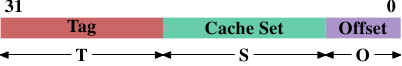
Figure 2.10: SDR SDRAM Operation
In Figure 2.10 the DRAM cell array can output the memory content at
the same rate it can be transported over the memory bus. If the DRAM
cell array can operate at 100MHz, the data transfer rate of the bus is thus
100Mb/s. The frequency f for all components is the same.
Increasing the throughput of the DRAM chip is expensive since the
energy consumption rises with the frequency. With a huge number of
array cells this is prohibitively expensive. {Power = Dynamic
Capacity Ч Voltage2 Ч Frequency.} In reality it is
even more of a problem since increasing the frequency usually also
requires increasing the voltage to maintain stability of the system.
DDR SDRAM (called DDR1
retroactively) manages to improve the throughput without increasing
any of the involved frequencies.
Figure 2.11: DDR1 SDRAM Operation
The difference between SDR and DDR1 is, as can be seen in
Figure 2.11 and guessed from the name, that twice the amount of
data is transported per cycle. I.e., the DDR1 chip transports data on
the rising and falling edge. This is sometimes called a
“double-pumped” bus. To make this possible without increasing the
frequency of the cell array a buffer has to be introduced. This
buffer holds two bits per data line. This in turn requires that, in
the cell array in Figure 2.7, the data bus consists of two
lines. Implementing this is trivial: one only has the use the same
column address for two DRAM cells and access them in parallel. The
changes to the cell array to implement this are also minimal.
The SDR
DRAMs were known simply by their frequency (e.g., PC100 for 100MHz
SDR). To make DDR1 DRAM sound better the marketers had to come up
with a new scheme since the frequency did not change. They came with
a name which contains the transfer rate in bytes a DDR module (they
have 64-bit busses) can sustain:
100MHz Ч 64bit Ч 2 = 1,600MB/s
Hence a DDR module with 100MHz frequency is called PC1600. With 1600
> 100 all marketing requirements are fulfilled; it sounds much
better although the improvement is really only a factor of
two. {I will take the factor of two but I do not have to like
the inflated numbers.}
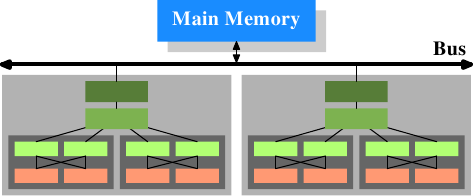
Figure 2.12: DDR2 SDRAM Operation
To get even more out of the memory technology DDR2 includes a bit more
innovation. The most obvious change that can be seen in
Figure 2.12 is the doubling of the frequency of the bus.
Doubling the frequency means doubling the bandwidth. Since this
doubling of the frequency is not economical for the cell array it is
now required that the I/O buffer gets four bits in each clock cycle
which it then can send on the bus. This means the changes to the DDR2
modules consist of making only the I/O buffer component of the DIMM
capable of running at higher speeds. This is certainly possible and
will not require measurably more energy, it is just one tiny component and
not the whole module. The names the marketers came up with for DDR2
are similar to the DDR1 names only in the computation of the value the
factor of two is replaced by four (we now have a quad-pumped bus).
Figure 2.13 shows the names of the modules in use today.
Array
Freq. |
Bus
Freq. |
Data
Rate |
Name
(Rate) |
Name
(FSB) |
| 133MHz | 266MHz | 4,256MB/s | PC2-4200 | DDR2-533 |
| 166MHz | 333MHz | 5,312MB/s | PC2-5300 | DDR2-667 |
| 200MHz | 400MHz | 6,400MB/s | PC2-6400 | DDR2-800 |
| 250MHz | 500MHz | 8,000MB/s | PC2-8000 | DDR2-1000 |
| 266MHz | 533MHz | 8,512MB/s | PC2-8500 | DDR2-1066 |
Figure 2.13: DDR2 Module Names
There is one more twist to the naming. The FSB speed used by CPU,
motherboard, and DRAM module is specified by using the
effective frequency. I.e., it factors in the transmission
on both flanks of the clock cycle and thereby inflates
the number. So, a 133MHz module with a 266MHz bus has an FSB
“frequency” of 533MHz.
The specification for DDR3 (the real one, not the fake GDDR3 used in
graphics cards) calls for more changes along the lines of the
transition to DDR2. The voltage will be reduced from 1.8V
for DDR2 to 1.5V for DDR3. Since the power consumption equation is
calculated using the square of the voltage this alone brings a
30% improvement. Add to this a reduction in die size plus other
electrical advances and DDR3 can manage, at the same frequency, to get
by with half the power consumption. Alternatively, with higher
frequencies, the same power envelope can be hit. Or with double the
capacity the same heat emission can be achieved.
The cell array of DDR3 modules will run at a quarter of the speed of
the external bus which requires an 8 bit I/O buffer, up from 4 bits
for DDR2. See Figure 2.14 for the schematics.
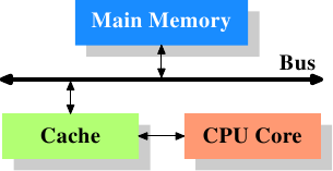
Figure 2.14: DDR3 SDRAM Operation
Initially DDR3 modules will likely have slightly higher CAS
latencies just because the DDR2 technology is more mature. This would
cause DDR3 to be useful only at frequencies which are higher than those
which can be achieved with DDR2, and, even then, mostly when bandwidth is more
important than latency. There is already talk about 1.3V modules
which can achieve the same CAS latency as DDR2. In any case, the
possibility of achieving higher speeds because of faster buses will
outweigh the increased latency.
One possible problem with DDR3 is that, for 1,600Mb/s transfer rate or
higher, the number of modules per channel may be reduced to just one.
In earlier versions this requirement held for all frequencies, so
one can hope that the requirement will at some point be lifted for all
frequencies. Otherwise the capacity of systems will be severely limited.
Figure 2.15 shows the names of the expected DDR3 modules.
JEDEC agreed so far on the first four types. Given that Intel's 45nm
processors have an FSB speed of 1,600Mb/s, the 1,866Mb/s is needed for
the overclocking market. We will likely see more of this towards the end
of the DDR3 lifecycle.
Array
Freq. |
Bus
Freq. |
Data
Rate |
Name
(Rate) |
Name
(FSB) |
| 100MHz | 400MHz | 6,400MB/s | PC3-6400 | DDR3-800 |
| 133MHz | 533MHz | 8,512MB/s | PC3-8500 | DDR3-1066 |
| 166MHz | 667MHz | 10,667MB/s | PC3-10667 | DDR3-1333 |
| 200MHz | 800MHz | 12,800MB/s | PC3-12800 | DDR3-1600 |
| 233MHz | 933MHz | 14,933MB/s | PC3-14900 | DDR3-1866 |
Figure 2.15: DDR3 Module Names
All DDR memory has one problem: the increased bus frequency makes it
hard to create parallel data busses. A DDR2 module has 240 pins. All
connections to data and address pins must be routed so that they have
approximately the same length. Even more of a problem is that, if more
than one DDR module is to be daisy-chained on the same bus, the signals
get more and more distorted for each additional module. The DDR2
specification allow only two modules per bus (aka channel), the DDR3
specification only one module for high frequencies. With 240 pins per
channel a single Northbridge cannot reasonably drive more than two
channels. The alternative is to have external memory controllers (as
in Figure 2.2) but this is expensive.
What this means is that commodity motherboards are restricted to hold
at most four DDR2 or DDR3 modules. This restriction severely limits the
amount of memory a system can have. Even old 32-bit IA-32 processors
can handle 64GB of RAM and memory demand even for home use is growing,
so something has to be done.
One answer is to add memory controllers into each processor as
explained in Section 2. AMD does it with the Opteron
line and Intel will do it with their CSI technology. This will help
as long as the reasonable amount of memory a processor is able to use
can be connected to a single processor. In some situations this is
not the case and this setup will introduce a NUMA architecture and its negative
effects. For some situations another solution is needed.
Intel's answer to this problem for big server machines, at least for
the next years, is called Fully
Buffered DRAM (FB-DRAM). The FB-DRAM modules use the same components
as today's DDR2 modules which makes them relatively cheap to produce.
The difference is in the connection with the memory controller.
Instead of a parallel data bus FB-DRAM utilizes a serial bus (Rambus
DRAM had this back when, too, and SATA is the successor of PATA, as is
PCI Express for PCI/AGP). The serial bus can be driven at a much
higher frequency, reverting negative impact of the serialization and
even increase the bandwidth. The main effects of using a serial bus
are
- more modules per channel can be used.
- more channels per Northbridge/memory controller can be used.
- the serial bus is designed to be fully-duplex (two lines).
An FB-DRAM module has only 69 pins, compared with the 240 for DDR2.
Daisy chaining FB-DRAM modules is much easier since the electrical
effects of the bus can be handled much better. The FB-DRAM
specification allows up to 8 DRAM modules per channel.
Compared with the connectivity requirements of a dual-channel
Northbridge it is now possible to drive 6 channels of FB-DRAM with
fewer pins: 2Ч240 pins versus 6Ч69 pins. The routing
for each channel is much simpler which could also help reducing the
cost of the motherboards.
Fully duplex parallel busses are prohibitively expensive for the
traditional DRAM modules, duplicating all those lines is too costly.
With serial lines (even if they are differential, as FB-DRAM requires)
this is not the case and so the serial bus is designed to be fully
duplexed, which means, in some situations, that the bandwidth is theoretically
doubled alone by this. But it is not the only place where parallelism
is used for bandwidth increase. Since an FB-DRAM controller can run
up to six channels at the same time the bandwidth can be increased
even for systems with smaller amounts of RAM by using FB-DRAM. Where
a DDR2 system with four modules has two channels, the same capacity can
handled via four channels using an ordinary FB-DRAM controller. The
actual bandwidth of the serial bus depends on the type of DDR2 (or
DDR3) chips used on the FB-DRAM module.
We can summarize the advantages like this:
| DDR2 | FB-DRAM |
|
| Pins | 240 | 69 |
| Channels | 2 | 6 |
| DIMMs/Channel | 2 | 8 |
| Max Memory | 16GB | 192GB |
| Throughput | ~10GB/s | ~40GB/s |
There are a few drawbacks to FB-DRAMs if multiple DIMMs on one channel
are used. The signal is delayed—albeit minimally—at each DIMM in the
chain, which means the latency increases. But for the same amount of
memory with the same frequency FB-DRAM can always be faster than DDR2
and DDR3 since only one DIMM per channel is needed; for large
memory systems DDR simply has no answer using commodity components.
2.2.5 Conclusions
This section should have shown that accessing DRAM is not an
arbitrarily fast process. At least not fast compared with the speed
the processor is running and with which it can access registers and
cache. It is important to keep in mind the differences between CPU and
memory frequencies. An Intel Core 2 processor running at 2.933GHz and a
1.066GHz FSB have a clock ratio of 11:1 (note: the 1.066GHz bus is
quad-pumped). Each stall of one cycle on the memory bus means a stall
of 11 cycles for the processor. For most machines the actual DRAMs
used are slower, thusly increasing the delay. Keep these numbers in
mind when we are talking about stalls in the upcoming sections.
The timing charts for the read command have shown that DRAM modules
are capable of high sustained data rates. Entire DRAM rows could be
transported without a single stall. The data bus could be kept
occupied 100%. For DDR modules this means two 64-bit words
transferred each cycle. With DDR2-800 modules and two channels this
means a rate of 12.8GB/s.
But, unless designed this way, DRAM access is not always sequential.
Non-continuous memory regions are used which means precharging and new
RAS signals are needed. This is when things slow down and when the
DRAM modules need help. The sooner the precharging can happen and the
RAS signal sent the smaller the penalty when the row is actually
used.
Hardware and software prefetching (see Section 6.3) can be used
to create more overlap in the timing and reduce the stall.
Prefetching also helps shift memory operations in time so that there
is less contention at later times, right before the data is actually
needed. This is a frequent problem when the data produced in one
round has to be stored and the data required for the next round has to be
read. By shifting the read in time, the write and read operations do
not have to be issued at basically the same time.
2.3 Other Main Memory Users
Beside the CPUs there are other system components which can access the
main memory. High-performance cards such as network and mass-storage
controllers cannot afford to pipe all the data they need or provide
through the CPU. Instead, they read or write the data directly from/to
the main memory (Direct Memory Access, DMA). In Figure 2.1
we can see that the cards can talk through the South- and Northbridge
directly with the memory. Other buses, like USB, also require FSB
bandwidth—even though they do not use DMA—since the Southbridge is
connected to the Northbridge through the FSB, too.
While DMA is certainly beneficial, it means that there is more
competition for the FSB bandwidth. In times with high DMA traffic the
CPU might stall more than usual while waiting for data from the main
memory. There are ways around this given the right hardware. With an
architecture as in Figure 2.3 one can make sure the computation
uses memory on nodes which are not affected by DMA. It is also
possible to attach a Southbridge to each node, equally
distributing the load on the FSB of all the nodes. There are a myriad
of possibilities. In Section 6 we will introduce techniques and
programming interfaces which help achieving the improvements which are
possible in software.
Finally it should be mentioned that some cheap systems have graphics
systems without separate, dedicated video RAM. Those systems use
parts of the main memory as video RAM. Since access to the video RAM
is frequent (for a 1024x768 display with 16 bpp at 60Hz we are talking
94MB/s) and system memory, unlike RAM on graphics cards, does not have
two ports this can substantially influence the systems performance
and especially the latency. It is best to ignore such systems
when performance is a priority. They are more trouble than they are worth.
People buying those machines know they will not get the best
performance.
Memory part 2: CPU caches
[Editor's note: This is the second installment in Ulrich Drepper's "What
every programmer should know about memory" document. Those who have not
read the first part will
likely want to start there. This is good stuff, and we once again thank
Ulrich for allowing us to publish it.
One quick request: in a document of this length there are bound to be a few
typographical errors remaining. If you find one, and wish to see it
corrected, please let us know via mail to lwn@lwn.net rather than by
posting a comment. That way we will be sure to incorporate the fix and get
it back into Ulrich's copy of the document and other readers will not have
to plow through uninteresting comments.]
CPUs are today much more sophisticated than they were only 25 years
ago. In those days, the frequency of the CPU core was at a level
equivalent to that of the memory bus. Memory access was only a bit slower
than register access. But this changed dramatically in the early
90s, when CPU designers increased the frequency of the CPU
core but the frequency of the memory bus and the performance of RAM
chips did not increase proportionally. This is not due to the fact
that faster RAM could not be built, as explained in the previous
section. It is possible but it is not economical. RAM as fast as current
CPU cores is orders of magnitude more expensive than any dynamic
RAM.
If the choice is between a machine with very little, very fast RAM and
a machine with a lot of relatively fast RAM, the second will always
win given a working set size which exceeds the small RAM size and the
cost of accessing secondary storage media such as hard drives. The
problem here is the speed of secondary storage, usually hard disks,
which must be used to hold the swapped out part of the working set.
Accessing those disks is orders of magnitude slower than even DRAM
access.
Fortunately it does not have to be an all-or-nothing decision. A
computer can have a small amount of high-speed SRAM in addition to the
large amount of DRAM. One possible implementation would be to
dedicate a certain area of the address space of the processor as
containing the SRAM and the rest the DRAM. The task of the operating
system would then be to optimally distribute data to make use of the
SRAM. Basically, the SRAM serves in this situation as an extension of
the register set of the processor.
While this is a possible implementation it is not viable. Ignoring
the problem of mapping the physical resources of such SRAM-backed
memory to the virtual address spaces of the processes (which by itself
is terribly hard) this approach would require each process to
administer in software the allocation of this memory region. The size
of the memory region can vary from processor to processor (i.e.,
processors have different amounts of the expensive SRAM-backed memory).
Each module which makes up part of a program will claim its share of the
fast memory, which introduces additional costs through synchronization
requirements. In short, the gains of having fast memory would be
eaten up completely by the overhead of administering the resources.
So, instead of putting the SRAM under the control of the OS or user, it
becomes a resource which is transparently used and administered by
the processors. In this mode, SRAM is used to make temporary copies of (to
cache, in other words) data in main memory which is likely to be used soon
by the processor. This is possible because program code and data has
temporal and spatial locality. This means that, over short periods of time,
there is a good chance that the same code or data gets reused. For
code this means that there are most likely loops in the code so that
the same code gets executed over and over again (the perfect case for
spatial locality). Data accesses are also ideally limited to
small regions. Even if the memory used over short time periods is not
close together there is a high chance that the same data will be reused before long
(temporal locality). For code this means, for instance, that
in a loop a function call is made and that function is located
elsewhere in the address space. The function may be distant in memory, but
calls to that function will be close in time. For data it means that the total
amount of memory used at one time (the working set size) is ideally
limited but the memory used, as a result of the random access
nature of RAM, is not close together. Realizing that locality
exists is key to the concept of CPU caches as we use them today.
A simple computation can show how effective caches can theoretically
be. Assume access to main memory takes 200 cycles and access to the
cache memory take 15 cycles. Then code using 100 data elements 100
times each will spend 2,000,000 cycles on memory operations if there is no
cache and only 168,500 cycles if all data can be cached. That is an
improvement of 91.5%.
The size of the SRAM used for caches is many times smaller than the
main memory. In the author's experience with workstations with CPU caches the
cache size has always been around 1/1000th of the size of the main memory
(today: 4MB cache and 4GB main memory). This alone does not
constitute a problem. If the size of the working set (the set of data
currently worked on) is smaller than the cache size it does not
matter. But computers do not have large main memories for no reason.
The working set is bound to be larger than the cache. This is especially true for
systems running multiple processes where the size of the working set is the sum of
the sizes of all the individual processes and the kernel.
What is needed to deal with the limited size of the cache is a set of good
strategies to determine what should be cached at any given time.
Since not all data of the working set is used at
exactly the same time we can use techniques to temporarily
replace some data in the cache with other data. And maybe this can be
done before the data is actually needed. This prefetching would
remove some of the costs of accessing main memory since it happens
asynchronously with respect to the execution of the program. All these techniques and
more can be used to make the cache appear bigger than it actually is.
We will discuss them in Section 3.3. Once all these
techniques are exploited it is up to the programmer to help the
processor. How this can be done will be discussed in Section 6.
3.1 CPU Caches in the Big Picture
Before diving into technical details of the implementation of CPU
caches some readers might find it useful to first see in some more
details how caches fit into the “big picture” of a modern computer
system.
Figure 3.1: Minimum Cache Configuration
Figure 3.1 shows the minimum cache configuration. It
corresponds to the architecture which could be found in early systems
which deployed CPU caches. The CPU core is no longer directly
connected to the main memory. {In even earlier systems the
cache was attached to the system bus just like the CPU and the main
memory. This was more a hack than a real solution.} All loads and
stores have to go through the cache. The connection between the CPU
core and the cache is a special, fast connection. In a simplified
representation, the main memory and the cache are connected to the
system bus which can also be used for communication with other
components of the system. We introduced the system bus as “FSB” which
is the name in use today; see Section 2.2. In this section we
ignore the Northbridge; it is assumed to be present to facilitate the
communication of the CPU(s) with the main memory.
Even though computers for the last several decades have used the von Neumann
architecture, experience has shown that it is of advantage to separate the
caches used for code and for data. Intel has used separate code and data
caches since 1993 and never looked back. The memory regions needed
for code and data are pretty much independent of each other, which is why independent
caches work better. In recent years another advantage emerged:
the instruction decoding step for the most common processors is
slow; caching decoded instructions can speed up the execution,
especially when the pipeline is empty due to incorrectly predicted or
impossible-to-predict branches.
Soon after the introduction of the cache the system got more
complicated. The speed difference between the cache and the main
memory increased again, to a point that another level of cache was
added, bigger and slower than the first-level cache. Only increasing
the size of the first-level cache was not an option for economical reasons.
Today, there are even machines with three levels of cache in regular
use. A system with such a processor looks like
Figure 3.2. With the increase on the number of cores in a
single CPU the number of cache levels might increase in future even
more.
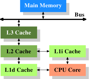
Figure 3.2: Processor with Level 3 Cache
Figure 3.2 shows three levels of cache and introduces the
nomenclature we will use in the remainder of the document. L1d is the
level 1 data cache, L1i the level 1 instruction cache, etc. Note that
this is a schematic; the data flow in reality need not pass through
any of the higher-level caches on the way from the core to the main
memory. CPU designers have a lot of freedom designing the interfaces
of the caches. For programmers these design choices are invisible.
In addition we have processors which have multiple cores and each core
can have multiple “threads”. The difference between a core and a
thread is that separate cores have separate copies of
(almost {Early multi-core processors even had separate
2nd level caches and no 3rd level cache.})
all the hardware resources. The cores can run completely
independently unless they are using the same resources—e.g., the
connections to the outside—at the same time. Threads, on the other
hand, share almost all of the processor's resources. Intel's implementation of
threads has only separate registers for the threads and even that is
limited, some registers are shared. The complete picture for a modern
CPU therefore looks like Figure 3.3.
Figure 3.3: Multi processor, multi-core, multi-thread
In this figure we have two processors, each with two cores, each of
which has two threads. The threads share the Level 1 caches. The
cores (shaded in the darker gray) have individual Level 1 caches. All
cores of the CPU share the higher-level caches. The two processors
(the two big boxes shaded in the lighter gray) of course do not share
any caches. All this will be important, especially when we are
discussing the cache effects on multi-process and multi-thread
applications.
3.2 Cache Operation at High Level
To understand the costs and savings of using a cache we have to
combine the knowledge about the machine architecture and RAM
technology from Section 2 with the structure of caches
described in the previous section.
By default all data read or written by the CPU cores is stored in
the cache. There are memory regions which cannot be cached but this
is something only the OS implementers have to be concerned about; it is not
visible to the application programmer. There are also instructions
which allow the programmer to deliberately bypass certain caches. This will be
discussed in Section 6.
If the CPU needs a data word the caches are searched first.
Obviously, the cache cannot contain the content of the entire
main memory (otherwise we would need no cache), but since all memory
addresses are cacheable, each cache entry is tagged using the
address of the data word in the main memory. This way a request to
read or write to an address can search the caches for a matching tag.
The address in this context can be either the virtual or physical
address, varying based on the cache implementation.
Since the tag requires space in addition to the actual memory, it is
inefficient to chose a word as the granularity of the cache. For a
32-bit word on an x86 machine the tag itself might need 32 bits or
more. Furthermore, since spatial locality is one of the principles on
which caches are based, it would be bad to not take this into account.
Since neighboring memory is likely to be used together it should also be
loaded into the cache together. Remember also what we
learned in Section 2.2.1: RAM modules are much more effective
if they can transport many data words in a row without a new CAS or
even RAS signal. So the entries stored in the caches are
not single words but, instead, “lines” of several contiguous words.
In early caches these lines were
32 bytes long; now the norm is 64 bytes. If the memory bus is
64 bits wide this means 8 transfers per cache line. DDR supports this
transport mode efficiently.
When memory content is needed by the processor the entire cache line
is loaded into the L1d. The memory address for each cache line is
computed by masking the address value according to the cache line
size. For a 64 byte cache line this means the low 6 bits are zeroed.
The discarded bits are used as the offset into the cache line. The remaining
bits are in some cases used to locate the line in the cache and as the tag.
In practice an address value is split into three parts. For a 32-bit
address it might look as follows:
With a cache line size of 2O
the low O bits are
used as the offset into the cache line. The next S bits
select the “cache set”. We will go into more detail soon on why
sets, and not single slots, are used for cache lines. For now it is
sufficient to understand there are 2S sets of cache lines.
This leaves the top 32 - S - O = T bits
which form the tag. These T bits are the value associated
with each cache line to distinguish all the
aliases {All cache lines with the same S part
of the address are known by the same alias.} which are
cached in the same cache set. The S bits used to address the
cache set do not have to be stored since they are the same for all
cache lines in the same set.
When an instruction modifies memory the processor still has to load a
cache line first because no instruction modifies an entire cache line
at once (exception to the rule: write-combining as explained in
Section 6.1). The content of the cache line before the write
operation therefore has to be loaded. It is not possible for a cache
to hold partial cache lines. A cache line which has been written to
and which has not been written back to main memory is said to be
“dirty”. Once it is written the dirty flag is cleared.
To be able to load new data in a cache it is almost always first
necessary to make room in the cache. An eviction from L1d pushes the
cache line down into L2 (which uses the same cache line size). This
of course means room has to be made in L2. This in turn might push the
content into L3 and ultimately into main memory. Each eviction is
progressively more expensive. What is described here is the model for an
exclusive cache as is preferred by modern AMD and VIA
processors. Intel implements inclusive caches {This
generalization is not completely correct. A few caches are exclusive
and some inclusive caches have exclusive cache properties.}
where each cache line
in L1d is also present in L2. Therefore evicting from L1d is much
faster. With enough L2 cache the disadvantage of wasting memory for
content held in two places is minimal and it pays off when evicting. A
possible advantage of an exclusive cache is that loading a new cache line
only has to touch the L1d and not the L2, which could be faster.
The CPUs are allowed to manage the caches as they like as long as the
memory model defined for the processor architecture is not changed.
It is, for instance, perfectly fine for a processor to take advantage of
little or no memory bus activity and proactively write dirty cache
lines back to main memory. The wide variety of cache architectures
among the processors for the x86 and x86-64, between manufacturers and
even within the models of the same manufacturer, are testament to the
power of the memory model abstraction.
In symmetric multi-processor (SMP) systems the caches of the CPUs
cannot work independently from each other. All processors are
supposed to see the same memory content at all times. The maintenance of
this uniform view of memory is called
“cache coherency”. If a processor were to look simply at its own caches
and main memory it would not see the content of dirty cache lines
in other processors. Providing direct access to the caches of one
processor from another processor would be terribly expensive and a
huge bottleneck. Instead, processors detect when another
processor wants to read or write to a certain cache line.
If a write access is detected and the processor has a clean copy of
the cache line in its cache, this cache line is marked invalid.
Future references will require the cache line to be reloaded. Note
that a read access on another CPU does not necessitate an
invalidation, multiple clean copies can very well be kept around.
More sophisticated cache implementations allow another possibility to
happen. If the cache line which another processor wants to read
from or write to is currently marked dirty in the first processor's cache
a different course of action is needed. In this case the main memory
is out-of-date and the requesting processor must, instead, get the cache line
content from the first processor. Through snooping, the first
processor notices this situation and automatically sends the
requesting processor the data. This action bypasses main memory, though
in some implementations the memory controller is supposed to notice
this direct transfer and store the updated cache line content in main
memory. If the access is for writing the first processor then
invalidates its copy of the local cache line.
Over time a number of cache coherency protocols have been developed. The
most important is MESI, which we will introduce in Section 3.3.4.
The outcome of all this can be summarized in a few simple
rules:
- A dirty cache line is not present in any other
processor's cache.
- Clean copies of the same cache line can reside in arbitrarily
many caches.
If these rules can be maintained, processors can use their
caches efficiently even in multi-processor systems. All the processors need to do
is to monitor each others' write accesses and compare the addresses
with those in their local caches. In the next section we will go
into a few more details about the implementation and especially the
costs.
Finally, we should at least give an impression of the costs associated
with cache hits and misses. These are the numbers Intel lists
for a Pentium M:
| To Where | Cycles |
|---|
| Register | <= 1 |
| L1d | ~3 |
| L2 | ~14 |
| Main Memory | ~240 |
These are the actual access times measured in CPU cycles. It is
interesting to note that for the on-die L2 cache a large part
(probably even the majority) of the access time is caused by wire delays.
This is a physical limitation which can only get worse with increasing
cache sizes. Only process shrinking (for instance, going from 60nm
for Merom to 45nm for Penryn in Intel's lineup) can improve those numbers.
The numbers in the table look high but, fortunately, the
entire cost does not have to be paid for each occurrence of the cache load and
miss. Some parts of the cost can be hidden. Today's processors all
use internal pipelines of different lengths where the instructions are
decoded and prepared for execution. Part of the preparation is
loading values from memory (or cache) if they are transferred to a
register. If the memory load operation can be started early enough in
the pipeline, it may happen in parallel with other operations and the
entire cost of the load might be hidden. This is
often possible for L1d; for some processors with long pipelines
for L2 as well.
There are many obstacles to starting the memory read early. It might be
as simple as not having sufficient resources for the memory access or
it might be that the final address of the load becomes available
late as the result of another instruction. In these cases the load
costs cannot be hidden (completely).
For write operations the CPU does not necessarily have to wait until
the value is safely stored in memory. As long as the execution of
the following instructions appears to have the same effect as if the
value were stored in memory there is nothing which prevents the CPU from
taking shortcuts. It can start executing the next instruction early.
With the help of shadow registers which can hold values no longer
available in a regular register it is even possible to change
the value which is to be stored in the incomplete write operation.
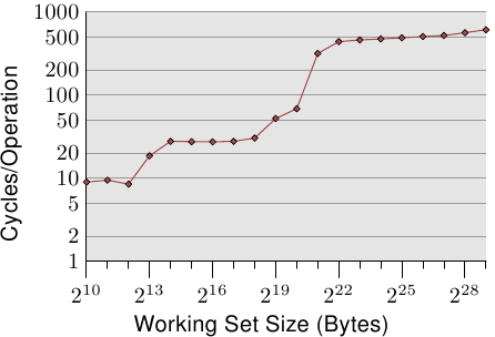
Figure 3.4: Access Times for Random Writes
For an illustration of the effects of cache behavior see Figure 3.4. We will talk about
the program which generated the data later; it is a simple simulation of
a program which accesses a configurable amount of memory repeatedly in
a random fashion. Each data item has a fixed size. The number of
elements depends on the selected working set size. The Y–axis shows
the average number of CPU cycles it takes to process one element;
note that the scale for the Y–axis is logarithmic. The same applies
in all the diagrams of this kind to the X–axis. The size of the
working set is always shown in powers of two.
The graph shows three distinct plateaus. This is not surprising: the
specific processor has L1d and L2 caches, but no L3. With some experience we can
deduce that the L1d is 213 bytes in size and that the L2 is
220 bytes in size. If the entire working set fits into the L1d
the cycles per operation on each element is below 10. Once the L1d
size is exceeded the processor has to load data from L2 and the average time
springs up to around 28. Once the L2 is not sufficient anymore the
times jump to 480 cycles and more. This is when many or most operations
have to load data from main memory. And worse: since data is
being modified dirty cache lines have to be written back, too.
This graph should give sufficient motivation to look into coding
improvements which help improve cache usage. We are not talking
about a few measly percent here; we are talking about orders-of-magnitude
improvements which are sometimes possible. In Section 6 we
will discuss techniques which allow writing more efficient code. The
next section goes into more details of CPU cache designs. The
knowledge is good to have but not necessary for the rest of the paper.
So this section could be skipped.
3.3 CPU Cache Implementation Details
Cache implementers have the problem that each cell in the huge main
memory potentially has to be cached. If the working set of a program
is large enough this means there are many main memory
locations which fight for each place in the cache. Previously it was
noted that a ratio of 1-to-1000 for cache versus main memory size is
not uncommon.
3.3.1 Associativity
It would be possible to implement a cache where each cache line can
hold a copy of any memory location. This is called a fully associative
cache. To access a cache line the processor core would have to
compare the tags of each and every cache line with the tag for the
requested address. The tag would be comprised of the entire part of
the address which is not the offset into the cache line (that means,
S in the figure on Section 3.2 is zero).
There are caches which are implemented like this
but, by looking at the numbers for an L2 in use today, will show that
this is impractical. Given a 4MB cache with 64B cache lines the cache
would have 65,536 entries. To achieve adequate performance the cache
logic would have to be able to pick from all these entries the one
matching a given tag in just a few cycles. The effort to implement
this would be enormous.
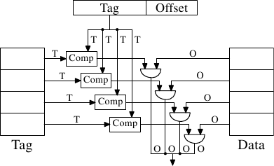
Figure 3.5: Fully Associative Cache Schematics
For each cache line a comparator is needed to compare the large tag
(note, S is zero). The letter next to each connection
indicates the width in bits. If none is given it is a single bit
line. Each comparator has to compare two T-bit-wide values.
Then, based on the result, the appropriate cache line content is
selected and made available. This requires merging as many sets of
O data lines as there are cache buckets. The number of
transistors needed to implement a single comparator is large
especially since it must work very fast. No iterative comparator is
usable. The only way to save on the number of comparators is to
reduce the number of them by iteratively comparing the tags. This is
not suitable for the same reason that iterative comparators are not:
it takes too long.
Fully associative caches are practical for small caches (for instance,
the TLB caches on some Intel processors are fully associative) but
those caches are small, really small. We are talking about a few dozen
entries at most.
For L1i, L1d, and higher level caches a different approach is needed.
What can be done is to restrict the search. In the most extreme
restriction each tag maps to exactly one cache entry. The computation
is simple: given the 4MB/64B cache with 65,536 entries we can directly
address each entry by using bits 5 to 21 of the address (16 bits).
The low 6 bits are the index into the cache line.
Figure 3.6: Direct-Mapped Cache Schematics
Such a direct-mapped cache is fast and relatively easy to
implement as can be seen in Figure 3.6. It requires
exactly one comparator, one multiplexer (two in this diagram where
tag and data are separated, but this is not a hard requirement on the
design), and some logic to select only valid cache line content. The
comparator is complex due to the speed requirements but there is only
one of them now; as a result more effort can be spent on making it fast. The real complexity
in this approach lies in the multiplexers. The number of transistors
in a simple multiplexer grows with O(log N), where N is the number of
cache lines. This is tolerable but might get slow, in which case speed
can be increased by spending more real estate on transistors in the multiplexers to
parallelize some of the work and to increase the speed. The total number of transistors can
grow slowly with a growing cache size which makes this solution very
attractive. But it has a drawback: it only works well if the
addresses used by the program are evenly distributed with respect to the
bits used for the direct mapping. If they are not, and this is
usually the case, some cache entries are heavily used and therefore
repeated evicted while others are hardly used at all or remain empty.
Figure 3.7: Set-Associative Cache Schematics
This problem can be solved by making the cache set associative.
A set-associative cache combines the features of the full associative
and direct-mapped caches to largely avoid the weaknesses of those designs.
Figure 3.7 shows the
design of a set-associative cache. The tag and data storage are divided into sets which are
selected by the address. This is similar to the direct-mapped cache.
But instead of only having one element for each set value in the cache
a small number of values is cached for the same set value. The tags
for all the set members is compared in parallel, which is similar to
the functioning of the fully associative cache.
The result is a cache which is not easily defeated by unfortunate or
deliberate selection of addresses with the same set numbers and at the
same time the size of the cache is not limited by the number of
comparators which can be implemented in parallel. If the cache grows
it is (in this figure) only the number of columns which increases, not the
number of rows. The number of rows only increases if the
associativity of the cache is increased. Today processors are using
associativity levels of up to 16 for L2 caches or higher. L1 caches
usually get by with 8.
L2
Cache
Size |
Associativity |
|---|
| Direct |
2 |
4 |
8 |
|---|
| CL=32 | CL=64 |
CL=32 | CL=64 |
CL=32 | CL=64 |
CL=32 | CL=64 |
|---|
| 512k
| 27,794,595 | 20,422,527 | 25,222,611 | 18,303,581 | 24,096,510 |
17,356,121 | 23,666,929 | 17,029,334 |
| 1M | 19,007,315 | 13,903,854 | 16,566,738 | 12,127,174 | 15,537,500 |
11,436,705 | 15,162,895 | 11,233,896 |
| 2M | 12,230,962 | 8,801,403 | 9,081,881 | 6,491,011 | 7,878,601 |
5,675,181 | 7,391,389 | 5,382,064 |
| 4M | 7,749,986 | 5,427,836 | 4,736,187 | 3,159,507 | 3,788,122 |
2,418,898 | 3,430,713 | 2,125,103 |
| 8M | 4,731,904 | 3,209,693 | 2,690,498 | 1,602,957 | 2,207,655 |
1,228,190 | 2,111,075 | 1,155,847 |
| 16M | 2,620,587 | 1,528,592 | 1,958,293 | 1,089,580 | 1,704,878 |
883,530 | 1,671,541 | 862,324 |
Table 3.1: Effects of Cache Size, Associativity, and Line Size
Given our 4MB/64B cache and 8-way set associativity the cache we are
left with has 8,192 sets and only 13 bits of the tag are used in
addressing the cache set. To determine which (if any) of the
entries in the cache set contains the addressed cache line 8 tags
have to be compared. That is feasible to do in very short time.
With an experiment we can see that this makes sense.
Table 3.1 shows the number of L2 cache misses for a
program (gcc in this case, the most important benchmark of them
all, according to the Linux kernel people) for changing cache size,
cache line size, and associativity set size. In Section 7.2 we
will introduce the tool to simulate the caches as required for this
test.
Just in case this is not yet obvious, the relationship of all these
values is that the cache size is
cache line size Ч associativity Ч number of sets
The addresses are mapped into the cache by using
O = log2 cache line size
S = log2 number of sets
in the way the figure in Section 3.2 shows.
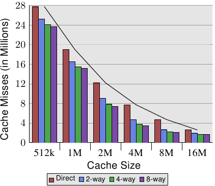
Figure 3.8: Cache Size vs Associativity (CL=32)
Figure 3.8 makes the data of the table more
comprehensible. It shows the data for a fixed cache line size of
32 bytes. Looking at the numbers for a given cache size we can see
that associativity can indeed help to reduce the number of cache
misses significantly. For an 8MB cache going from direct mapping to
2-way set associative cache saves almost 44% of the cache misses. The
processor can keep more of the working set in the cache with a set
associative cache compared with a direct mapped cache.
In the literature one can occasionally read that introducing
associativity has the same effect as doubling cache size. This is
true in some extreme cases as can be seen in the jump from the 4MB to
the 8MB cache. But it certainly is not true for further doubling of
the associativity. As we can see in the data, the successive gains
are much smaller. We should not completely discount the effects,
though. In the example program the peak memory use is 5.6M. So with
a 8MB cache there are unlikely to be many (more than two) uses for the
same cache set. With a larger working set the savings can be higher
as we can see from the larger benefits of associativity for the smaller
cache sizes.
In general, increasing the associativity of a cache above 8 seems to
have little effects for a single-thread workload. With the
introduction of multi-core processors which use a shared L2 the
situation changes. Now you basically have two programs hitting on the
same cache which causes the associativity in practice to be halved (or
quartered for quad-core processors). So it can be expected that, with
increasing numbers of cores, the associativity of the shared caches
should grow. Once this is not possible anymore (16-way set associativity is
already hard) processor designers have to start using shared L3 caches and
beyond, while L2 caches are potentially shared by a subset of the cores.
Another effect we can study in Figure 3.8 is how
the increase in cache size helps with performance. This data
cannot be interpreted without knowing about the working set size.
Obviously, a cache as large as the main memory would lead to better
results than a smaller cache, so there is in general no limit to the
largest cache size with measurable benefits.
As already mentioned above, the size of the working set at its peak is
5.6M. This does not give us any absolute number of the maximum
beneficial cache size but it allows us to estimate the number. The
problem is that not all the memory used is contiguous and, therefore,
we have, even with a 16M cache and a 5.6M working set, conflicts (see the
benefit of the 1-way set associative 16MB cache over the direct mapped
version). But it is a safe bet that with the same workload the
benefits of a 32MB cache would be negligible. But who says the
working set has to stay the same? Workloads are growing over time
and so should the cache size. When buying machines, and one has to
choose the cache size one is willing to pay for, it is worthwhile to
measure the working set size. Why this is important can be seen in
the figures on Figure 3.10.
Figure 3.9: Test Memory Layouts
Two types of tests are run. In the first test the elements are
processed sequentially. The test program follows the pointer n
but the array elements are chained so that they are traversed in the
order in which they are found in memory. This can be seen in the
lower part of Figure 3.9. There is one back reference
from the last element. In the second test (upper part of the figure)
the array elements are traversed in a random order. In both cases the
array elements form a circular single-linked list.
3.3.2 Measurements of Cache Effects
All the figures are created by measuring a program which can simulate
working sets of arbitrary size, read and write access, and sequential
or random access. We have already seen some results in
Figure 3.4. The program creates an array corresponding to
the working set size of elements of this type:
  struct l {
     struct l *n;
     long int pad[NPAD];
   };
All entries are chained in a circular list using the n element,
either in sequential or random order. Advancing from one entry to the
next always uses the pointer, even if the elements are laid out
sequentially. The pad element is the payload and it can grow
arbitrarily large. In some tests the data is modified, in others the
program only performs read operations.
In the performance measurements we are talking about working set
sizes. The working set is made up of an array of struct l
elements. A working set of 2N bytes contains
2N/sizeof(struct l)
elements. Obviously sizeof(struct l) depends on the value of
NPAD. For 32-bit systems, NPAD=7 means the size of each
array element is 32 bytes, for 64-bit systems the size is 64 bytes.
Single Threaded Sequential Access
The simplest case is a simple walk over all the entries in the list.
The list elements are laid out sequentially, densely packed. Whether
the order of processing is forward or backward does not matter, the
processor can deal with both directions equally well.
What we measure here—and in all the following tests—is how long it
takes to handle a single list element. The time unit is a processor
cycle. Figure 3.10 shows the result. Unless otherwise
specified, all measurements are made on a Pentium 4 machine in 64-bit
mode which means the structure l with NPAD=0 is eight bytes
in size.
Figure 3.10: Sequential Read Access, NPAD=0
Figure 3.11: Sequential Read for Several Sizes
The first two measurements are polluted by noise. The measured
workload is simply too small to filter the effects of the rest of the
system out. We can safely assume that the values are all at the
4 cycles level. With this in mind we can see three distinct levels:
- Up to a working set size of 214 bytes.
- From 215 bytes to 220 bytes.
- From 221 bytes and up.
These steps can be easily explained: the processor has a 16kB L1d and
1MB L2. We do not see sharp edges in the transition from one level to
the other because the caches are used by other parts of the system as
well and so the cache is not exclusively available for the
program data. Specifically the L2 cache is a unified cache and also
used for the instructions (NB: Intel uses inclusive caches).
What is perhaps not quite expected are the actual times for the
different working set sizes. The times for the L1d hits are
expected: load times after an L1d hit are around 4 cycles on the
P4. But what about the L2 accesses? Once the L1d is not sufficient
to hold the data one might expect it would take 14 cycles or more per
element since this is the access time for the L2. But the results show
that only about 9 cycles are required. This discrepancy can be explained by the
advanced logic in the processors. In anticipation of using
consecutive memory regions, the processor prefetches the next
cache line. This means that when the next line is actually used it is
already halfway loaded. The delay required to wait for the next cache
line to be loaded is therefore much less than the L2 access time.
The effect of prefetching is even more visible once the working set size grows beyond the
L2 size. Before we said that a main memory access takes 200+ cycles.
Only with effective prefetching is it possible for the processor to
keep the access times as low as 9 cycles. As we can see from the
difference between 200 and 9, this works out nicely.
We can observe the processor while prefetching, at least indirectly. In
Figure 3.11 we see the times for the same working set sizes
but this time we see the graphs for different sizes of the structure
l. This means we have fewer but larger elements in the list.
The different sizes have the effect that the distance
between the n elements in the (still consecutive) list grows.
In the four cases of the graph the distance is 0, 56, 120, and 248 bytes
respectively.
At the bottom we can see the line from the previous graph, but this
time it appears more or less as a flat line. The times for the other cases are
simply so much worse. We can see in this graph, too, the three
different levels and we see the large errors in the tests with the
small working set sizes (ignore them again). The lines more or less
all match each other as long as only the L1d is involved. There is no
prefetching necessary so all element sizes just hit the L1d for each
access.
For the L2 cache hits we see that the three new lines all pretty much
match each other but that they are at a higher level (about 28). This
is the level of the access time for the L2. This means prefetching
from L2 into L1d is basically disabled. Even with NPAD=7 we
need a new cache line for each iteration of the loop; for
NPAD=0, instead, the loop has to iterate eight times before the next cache
line is needed. The prefetch logic cannot load a new cache line every
cycle. Therefore we see a stall to load from L2 in every iteration.
It gets even more interesting once the working set size exceeds the L2
capacity. Now all four lines vary widely. The different element
sizes play obviously a big role in the difference in performance.
The processor should recognize the size of the strides and not fetch
unnecessary cache lines for NPAD=15 and 31 since the element size
is smaller than the prefetch window (see
Section 6.3.1). Where the element size is hampering
the prefetching efforts is a result of a limitation of hardware prefetching: it
cannot cross page boundaries. We are reducing the effectiveness of
the hardware scheduler by 50% for each size increase. If the
hardware prefetcher were
allowed to cross page boundaries and the next page is not resident or valid the OS
would have to get involved in locating the page. That means the program
would experience a page fault it did not initiate itself. This is
completely unacceptable since the processor does not know whether a
page is not present or does not exist. In the latter case the OS
would have to abort the process. In any case, given that, for NPAD=7
and higher, we need one cache line per list element the hardware
prefetcher cannot do much. There simply is no time to load the data
from memory since all the processor does is read one word and then
load the next element.
Another big reason for the slowdown are the misses of the TLB cache.
This is a cache where the results of the translation of a
virtual address to a physical address are stored, as is explained
in more detail in Section 4. The TLB cache is quite small
since it has to be extremely fast. If more pages are accessed
repeatedly than the TLB cache has entries for the translation from
virtual to physical address has to be constantly repeated. This is a
very costly operation. With larger element sizes the cost of a TLB
lookup is amortized over fewer elements. That means the total number
of TLB entries which have to be computed per list element is higher.
To observe the TLB effects we can run a different test. For one
measurement we lay out the elements sequentially as usual. We use
NPAD=7 for elements which occupy one entire cache line. For
the second measurement we place each list element on a separate page.
The rest of each page is left untouched and we do not count it in
the total for the working set size. {Yes, this is a bit
inconsistent because in the other tests we count the unused part of
the struct in the element size and we could define NPAD so that
each element fills a page. In that case the working set sizes would
be very different. This is not the point of this test, though, and
since prefetching is ineffective anyway this makes little
difference.} The consequence is that, for the first measurement, each
list iteration requires a new cache line and, for every 64
elements, a new page. For the second measurement each iteration
requires loading a new cache line which is on a new page.
Figure 3.12: TLB Influence for Sequential Read
The result can be seen in Figure 3.12. The measurements were
performed on the same machine as Figure 3.11. Due to
limitations of the available RAM the working set size had to be
restricted to 224 bytes which requires 1GB to place the objects
on separate pages. The lower, red curve corresponds exactly to the
NPAD=7 curve in Figure 3.11. We see the distinct
steps showing the sizes of the L1d and L2 caches. The second curve
looks radically different. The important feature is the huge spike
starting when the working set size reaches 213 bytes. This is
when the TLB cache overflows. With an element size of 64 bytes we
can compute that the TLB cache has 64 entries. There are no page
faults affecting the cost since the program locks the memory to prevent
it from being swapped out.
As can be seen the number of cycles it takes to compute the physical
address and store it in the TLB is very high. The graph in
Figure 3.12 shows the extreme case, but it should now be clear
that a significant factor in the slowdown for larger NPAD values is
the reduced efficiency of the TLB cache. Since the physical address
has to be computed before a cache line can be read for either L2 or
main memory the address translation penalties are additive to the memory access times. This in
part explains why the total cost per list element for NPAD=31
is higher than the theoretical access time for the RAM.
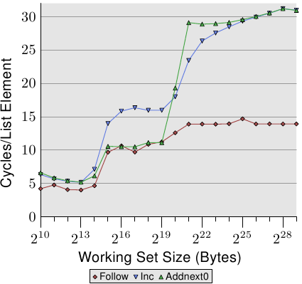
Figure 3.13: Sequential Read and Write, NPAD=1
We can glimpse a few more details of the prefetch implementation by
looking at the data of test runs where the list elements are modified.
Figure 3.13 shows three lines. The element width is in all
cases 16 bytes. The first line is the now familiar list walk which
serves as a baseline. The second line, labeled “Inc”, simply
increments the pad[0] member of the current element before going
on to the next. The third line, labeled “Addnext0”, takes the
pad[0] list element of the next element and adds it to
the pad[0] member of the current list element.
The naпve assumption would be that the “Addnext0” test runs slower
because it has more work to do. Before advancing to the next list
element a value from that element has to be loaded. This is why it is
surprising to see that this test actually runs, for some working set
sizes, faster than the “Inc” test. The explanation for this is that
the load from the next list element is basically a forced prefetch.
Whenever the program advances to the next list element we know for
sure that element is already in the L1d cache. As a result we see
that the “Addnext0” performs as well as the simple “Follow” test
as long as the working set size fits into the L2 cache.
The “Addnext0” test runs out of L2 faster than the “Inc” test,
though. It needs more data loaded from main memory. This is why the
“Addnext0” test reaches the 28 cycles level for a working
set size of 221 bytes. The 28 cycles level is twice as high as
the 14 cycles level the “Follow” test reaches. This is easy to
explain, too. Since the other two tests modify memory an L2 cache
eviction to make room for new cache lines cannot simply discard the
data. Instead it has to be written to memory. This means the
available bandwidth on the FSB is cut in half, hence doubling the time
it takes to transfer the data from main memory to L2.
Figure 3.14: Advantage of Larger L2/L3 Caches
One last aspect of the sequential, efficient cache handling is the
size of the cache. This should be obvious but it still should be
pointed out. Figure 3.14 shows the timing for the
Increment benchmark with 128-byte elements (NPAD=15 on 64-bit machines).
This time we see the measurement from three different machines. The
first two machines are P4s, the last one a Core2 processor. The first
two differentiate themselves by having different cache sizes. The
first processor has a 32k L1d and an 1M L2. The second one has 16k
L1d, 512k L2, and 2M L3. The Core2 processor has 32k L1d and 4M L2.
The interesting part of the graph is not necessarily how well the
Core2 processor performs relative to the other two (although it is
impressive). The main point of interest here is the region where the
working set size is too large for the respective last level cache and
the main memory gets heavily involved.
Set
Size |
Sequential |
Random |
|---|
| L2 Hit |
L2 Miss |
#Iter |
Ratio Miss/Hit |
L2 Accesses Per Iter |
L2 Hit |
L2 Miss |
#Iter |
Ratio Miss/Hit |
L2 Accesses Per Iter |
|---|
| 220 | 88,636 | 843 | 16,384 | 0.94% | 5.5 | 30,462 | 4721 | 1,024 | 13.42% | 34.4 |
| 221 | 88,105 | 1,584 | 8,192 | 1.77% | 10.9 | 21,817 | 15,151 | 512 | 40.98% | 72.2 |
| 222 | 88,106 | 1,600 | 4,096 | 1.78% | 21.9 | 22,258 | 22,285 | 256 | 50.03% |
174.0 |
| 223 | 88,104 | 1,614 | 2,048 | 1.80% | 43.8 | 27,521 | 26,274 | 128 | 48.84% |
420.3 |
| 224 | 88,114 | 1,655 | 1,024 | 1.84% | 87.7 | 33,166 | 29,115 | 64 | 46.75% | 973.1 |
| 225 | 88,112 | 1,730 | 512 | 1.93% | 175.5 | 39,858 | 32,360 | 32 | 44.81% | 2,256.8 |
| 226 | 88,112 | 1,906 | 256 | 2.12% | 351.6 | 48,539 | 38,151 | 16 | 44.01% | 5,418.1 |
| 227 | 88,114 | 2,244 | 128 | 2.48% | 705.9 | 62,423 | 52,049 | 8 | 45.47% | 14,309.0 |
| 228 | 88,120 | 2,939 | 64 | 3.23% | 1,422.8 | 81,906 | 87,167 | 4 |
51.56% | 42,268.3 |
| 229 | 88,137 | 4,318 | 32 | 4.67% | 2,889.2 | 119,079 | 163,398 | 2 | 57.84% |
141,238.5 |
Table 3.2: L2 Hits and Misses for Sequential and Random Walks, NPAD=0
As expected, the larger the last level cache is the longer the curve
stays at the low level corresponding to the L2 access costs. The
important part to notice is the performance advantage this provides.
The second processor (which is slightly older) can perform the work on
the working set of 220 bytes twice as fast as the first
processor. All thanks to the increased last level cache size. The
Core2 processor with its 4M L2 performs even better.
For a random workload this might not mean that much. But if the
workload can be tailored to the size of the last level cache the
program performance can be increased quite dramatically. This is why
it sometimes is worthwhile to spend the extra money for
a processor with a larger cache.
Single Threaded Random Access Measurements
We have seen that the processor is able to hide most of the main
memory and even L2 access latency by prefetching cache lines into L2
and L1d. This can work well only when the memory access is
predictable, though.
Figure 3.15: Sequential vs Random Read, NPAD=0
If the access is unpredictable or random the situation is quite
different. Figure 3.15 compares the per-list-element times
for the sequential access (same as in Figure 3.10) with the
times when the list elements are randomly distributed in the working
set. The order is determined by the linked list which is randomized.
There is no way for the processor to reliably prefetch data. This can
only work by chance if elements which are used shortly after one
another are also close to each other in memory.
There are two important points to note in Figure 3.15.
First, the large number is cycles needed for growing working set
sizes. The machine makes it possible to access the main memory in
200-300 cycles but here we reach 450 cycles and more. We have seen
this phenomenon before (compare Figure 3.11). The
automatic prefetching is actually working to a disadvantage here.
The second interesting point is that the curve is not flattening at
various plateaus as it has been for the sequential access cases. The
curve keeps on rising. To explain this we can measure the L2 access
of the program for the various working set sizes. The result can be
seen in Figure 3.16 and Table 3.2.
The figure shows the when the working set size is larger than the L2
size the cache miss ratio (L2 misses / L2 access) starts to
grow. The curve has a similar form to the one in
Figure 3.15: it rises quickly, declines slightly, and
starts to rise again. There is a strong correlation with the cycles
per list element graph. The L2 miss rate will grow until it
eventually reaches close to 100%. Given a large enough working set
(and RAM) the probability that any of the randomly picked cache lines
is in L2 or is in the process of being loaded can be reduced
arbitrarily.
The increasing cache miss rate alone explains some of the costs. But
there is another factor. Looking at Table 3.2 we can
see in the L2/#Iter columns that the total number of L2 uses per
iteration of the program is growing. Each working set is twice as
large as the one before. So, without caching we would expect double
the main memory accesses. With caches and (almost) perfect
predictability we see the modest increase in the L2 use shown in the
data for sequential access. The increase is due to the increase of
the workspace set size and nothing else.
Figure 3.16: L2d Miss Ratio
Figure 3.17: Page-Wise Randomization, NPAD=7
For random access the per-element time increases by more than 100%
for each doubling of the working set size. This means the average
access time per list element increases since the working set size only
doubles. The reason behind this is a rising rate of TLB misses.
In Figure 3.17 we see the cost for random accesses for
NPAD=7. Only this time the randomization is modified. While in the
normal case the entire list of randomized as one block (indicated by
the label ∞) the other 11 curves show randomizations which are
performed in smaller blocks. For the curve labeled '60' each set of
60 pages (245.760 bytes) is randomized individually. That means all
list elements in block are traversed before going over to an element
in the next block. This has the effect that number of TLB entries
which are used at any one time is limited.
The element size for NPAD=7 is 64 bytes, which corresponds to the cache
line size. Due to the randomized order of the list elements it is
unlikely that the hardware prefetcher has any effect, most certainly
not for more than a handful of elements. This means the L2 cache miss
rate does not differ significantly from the randomization of the
entire list in one block. The performance of the test with
increasing block size approaches asymptotically the curve for the
one-block randomization. This means the performance of this latter
test case is significantly influenced by the TLB misses. If the TLB
misses can be lowered the performance increases significantly (in one
test we will see later up to 38%).
3.3.3 Write Behavior
Before we start looking at the cache behavior when multiple execution
contexts (threads or processes) use the same memory we have to explore
a detail of cache implementations. Caches are
supposed to be coherent and this coherency is supposed to be completely
transparent for the userlevel code. Kernel code is a different story;
it occasionally requires cache flushes.
This specifically means that, if a cache line is modified, the result
for the system after this point in time is the same as if there were
no cache at all and the main memory location itself had been
modified. This can be implemented in two ways or policies:
- write-through cache implementation;
- write-back cache implementation.
The write-through cache is the simplest way to implement cache
coherency. If the cache line is written to, the processor immediately
also writes the cache line into main memory. This ensures that, at
all times, the main memory and cache are in sync. The cache content
could simply be discarded whenever a cache line is replaced. This
cache policy is simple but not very fast. A program which, for
instance, modifies a local variable over and over again would create a
lot of traffic on the FSB even though the data is likely not used
anywhere else and might be short-lived.
The write-back policy is more sophisticated. Here the processor does
not immediately write the modified cache line back to main
memory. Instead, the cache line is only marked as dirty. When the cache line
is dropped from the cache at some point in the future the dirty bit will
instruct the processor to write the data back at that time instead of
just discarding the content.
Write-back caches have the chance to be significantly better
performing, which is why most memory in a system with a decent
processor is cached this way. The processor can even take advantage
of free capacity on the FSB to store the content of a cache line
before the line has to be evacuated. This allows the dirty bit to be
cleared and the processor can just drop the cache line when the room
in the cache is needed.
But there is a significant problem with the write-back
implementation. When more than one processor (or core or
hyper-thread) is available and accessing the same memory it must still
be assured that both processors see the same memory content at all
times. If a cache line is dirty on one processor (i.e., it has not been
written back yet) and a second processor tries to read the same memory
location, the read operation cannot just go out to the main memory.
Instead the content of the first processor's cache line is needed. In
the next section we will see how this is currently implemented.
Before we get to this there are two more cache policies to mention:
- write-combining; and
- uncacheable.
Both these policies are used for special regions of the address
space which are not backed by real RAM. The kernel sets up these
policies for the address ranges (on x86 processors using the Memory
Type Range Registers, MTRRs) and the rest happens automatically. The
MTRRs are also usable to select between write-through and write-back
policies.
Write-combining is a limited caching optimization more often used for RAM on
devices such as graphics cards. Since the transfer costs to the
devices are much higher than the local RAM access it is even more
important to avoid doing too many transfers. Transferring an entire cache line
just because a word in the line has been written is wasteful if the next operation
modifies the next word. One can easily imagine that this is a common
occurrence, the memory for horizontal neighboring pixels on a screen
are in most cases neighbors, too. As the name suggests,
write-combining combines multiple write accesses before the cache line
is written out. In ideal cases the entire cache line is modified word
by word and, only after the last word is written, the cache line is
written to the device. This can speed up access to RAM on devices
significantly.
Finally there is uncacheable memory. This usually means the memory
location is not backed by RAM at all. It might be a special address
which is hardcoded to have some functionality outside the CPU. For
commodity hardware this most often is the case for memory mapped
address ranges which translate to accesses to cards and devices
attached to a bus (PCIe etc). On embedded boards one sometimes finds
such a memory address which can be used to turn an LED on and off.
Caching such an address would obviously be a bad idea. LEDs in this
context are used for debugging or status reports and one wants to see
this as soon as possible. The memory on PCIe cards can change
without the CPU's interaction, so this memory should not be cached.
3.3.4 Multi-Processor Support
In the previous section we have already pointed out the problem we have
when multiple processors come into play. Even multi-core processors
have the problem for those cache levels which are not shared (at least
the L1d).
It is completely impractical to provide direct access from one
processor to the cache of another processor. The connection is simply
not fast enough, for a start. The practical alternative is to
transfer the cache content over to the other processor in case it is
needed. Note that this also applies to caches which are not shared on
the same processor.
The question now is when does this cache line transfer have to happen?
This question is pretty easy to answer: when one processor needs a
cache line which is dirty in another processor's cache for reading or
writing. But how can a processor determine whether a cache line is
dirty in another processor's cache? Assuming it is just because a cache
line is loaded by another processor would be suboptimal (at best).
Usually the majority of memory accesses are read accesses and the resulting
cache lines are not dirty. Processor operations on cache lines
are frequent (of course, why else would we have this paper?) which means
broadcasting information about changed cache lines after each
write access would be impractical.
What developed over the years is the MESI cache coherency protocol
(Modified, Exclusive, Shared, Invalid). The protocol is named after
the four states a cache line can be in when using the MESI protocol:
- Modified: The local processor has modified the cache line.
This also implies it is the only copy in any cache.
- Exclusive: The cache line is not modified but known to not be
loaded into any other processor's cache.
- Shared: The cache line is not modified and might exist in
another processor's cache.
- Invalid: The cache line is invalid, i.e., unused.
This protocol developed over the years from simpler versions which
were less complicated but also less efficient. With these four states
it is possible to efficiently implement write-back caches while also
supporting concurrent use of read-only data on different processors.
Figure 3.18: MESI Protocol Transitions
The state changes are accomplished without too much effort by the
processors listening, or snooping, on the other processors' work.
Certain operations a processor performs are announced on external pins
and thus make the processor's cache handling visible to the outside. The
address of the cache line in question is visible on the address bus.
In the following description of the states and their transitions
(shown in Figure 3.18) we will point out when the bus is involved.
Initially all cache lines are empty and hence also Invalid. If data is
loaded into the cache for writing the cache changes to Modified. If
the data is loaded for reading the new state depends on whether
another processor has the cache line loaded as well. If this is the case
then the new state is Shared, otherwise Exclusive.
If a Modified cache line is read from or written to on the local
processor, the instruction can use the current cache content and the
state does not change. If a second processor wants to read from the
cache line the first processor has to send the content of its cache
to the second processor and then it can change the state to Shared. The
data sent to the second processor is also received and processed by
the memory controller which stores the content in memory. If this
did not happen the cache line could not be marked as Shared. If
the second processor wants to write to the cache line the first
processor sends the cache line content and marks the cache line
locally as Invalid. This is the infamous
“Request For Ownership” (RFO) operation. Performing this operation
in the last level cache, just like the I→M transition is
comparatively expensive. For write-through caches we also
have to add the time it takes to write the new cache line content to
the next higher-level cache or the main memory, further increasing the
cost.
If a cache line is in the Shared state and the local processor reads
from it no state change is necessary and the read request can be
fulfilled from the cache. If the cache line is locally written to the
cache line can be used as well but the state changes to Modified. It
also requires that all other possible copies of the cache line in
other processors are marked as Invalid. Therefore the write operation
has to be announced to the other processors via an RFO message. If
the cache line is requested for reading by a second processor nothing
has to happen. The main memory contains the current data and the
local state is already Shared. In case a second processor wants to
write to the cache line (RFO) the cache line is simply marked Invalid.
No bus operation is needed.
The Exclusive state is mostly identical to the Shared state with one
crucial difference: a local write operation does not have to be
announced on the bus. The local cache copy is known to be the only one.
This can be a huge advantage so the processor will try to keep as many
cache lines as possible in the Exclusive state instead of the Shared
state. The latter is the fallback in case the information is not
available at that moment. The Exclusive state can also be left out
completely without causing functional problems. It is only the
performance that will suffer since the E→M transition is
much faster than the S→M transition.
From this description of the state transitions it should be clear
where the costs specific to multi-processor operations are. Yes,
filling caches is still expensive but now we also have to look out for
RFO messages. Whenever such a message has to be sent things are going to
be slow.
There are two situations when RFO messages are necessary:
- A thread is migrated from one processor to another and all the
cache lines have to be moved over to the new processor once.
- A cache line is truly needed in two different processors.
{At a
smaller level the same is true for two cores on the same processor.
The costs are just a bit smaller. The RFO message is likely to be
sent many times.}
In multi-thread or multi-process programs there is always some need
for synchronization; this synchronization is implemented using memory.
So there are some valid RFO messages. They still have to be kept as
infrequent as possible. There are other sources of RFO messages,
though. In Section 6 we will explain these scenarios. The
Cache coherency protocol messages must be distributed among the
processors of the system. A MESI transition cannot happen until it
is clear that all the processors in the system have had a chance to reply
to the message. That means that the longest possible time a reply can
take determines the speed of the coherency protocol. {Which is
why we see nowadays, for instance, AMD Opteron systems with three
sockets. Each processor is exactly one hop away given that the
processors only have three hyperlinks and one is needed for the
Southbridge connection.} Collisions on the bus are possible, latency
can be high in NUMA systems, and of course sheer traffic volume can
slow things down. All good reasons to focus on avoiding unnecessary
traffic.
There is one more problem related to having more than one processor in
play. The effects are highly machine specific but in principle the
problem always exists: the FSB is a shared resource. In most
machines all processors are connected via one single bus to the memory
controller (see Figure 2.1). If a single processor can
saturate the bus (as is usually the case) then two or four
processors sharing the same bus will restrict the bandwidth available
to each processor even more.
Even if each processor has its own bus to the memory controller as in
Figure 2.2 there is still the bus to the memory modules.
Usually this is one bus but, even in the extended model in
Figure 2.2, concurrent accesses to the same memory module will
limit the bandwidth.
The same is true with the AMD model where each processor can have
local memory. Yes, all processors can concurrently access their local
memory quickly. But multi-thread and multi-process programs--at least
from time to time--have to access the same memory regions to
synchronize.
Concurrency is severely limited by the finite bandwidth available for
the implementation of the necessary synchronization. Programs need to
be carefully designed to minimize accesses from different processors
and cores to the same memory locations. The following measurements
will show this and the other cache effects related to multi-threaded
code.
Multi Threaded Measurements
To ensure that the gravity of the problems introduced by concurrently
using the same cache lines on different processors is understood, we will
look here at some more performance graphs for the same program we used
before. This time, though, more than one thread is running at the same
time. What is measured is the fastest runtime of any of the threads.
This means the time for a complete run when all threads are done is
even higher. The machine used has four processors; the tests use
up to four threads. All processors share one bus to the memory
controller and there is only one bus to the memory modules.
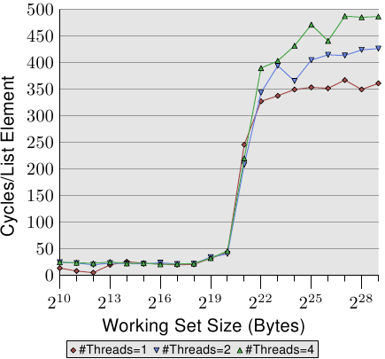
Figure 3.19: Sequential Read Access, Multiple Threads
Figure 3.19 shows the performance for sequential read-only
access for 128 bytes entries (NPAD=15 on 64-bit machines). For the
curve for one thread we can expect a curve similar to
Figure 3.11. The measurements are for a different machine so
the actual numbers vary.
The important part in this figure is of course the behavior when
running multiple threads. Note that no memory is modified and no
attempts are made to keep the threads in sync when walking the linked
list. Even though no RFO messages are necessary and all the cache lines
can be shared, we see up to an 18% performance decrease for the fastest
thread when two threads are used and up to 34% when four threads are
used. Since no cache lines have to be transported between the
processors this slowdown is solely caused by one or both of the
two bottlenecks: the shared bus from the processor to the memory
controller and bus from the memory controller to the memory modules.
Once the working set size is larger than the L3 cache in this machine
all three threads will be prefetching new list elements. Even with two
threads the available bandwidth is not sufficient to scale linearly
(i.e., have no penalty from running multiple threads).
When we modify memory things get even uglier. Figure 3.20
shows the results for the sequential Increment test.
Figure 3.20: Sequential Increment, Multiple Threads
This graph is
using a logarithmic scale for the Y axis. So, do not be fooled by
the apparently small differences. We still have about a 18% penalty
for running two threads and now an amazing 93% penalty for running four threads.
This means the prefetch traffic together with the write-back
traffic is pretty much saturating the bus when four threads are used.
We use the logarithmic scale to show the results for the L1d range.
What can be seen is that, as soon as more than one thread is running,
the L1d is basically ineffective. The single-thread access times exceed 20
cycles only when the L1d is not sufficient to hold the working set. When
multiple threads are running, those access times are hit immediately, even
with the smallest working set sizes.
One aspect of the problem is not shown here. It is hard to measure
with this specific test program. Even though the test modifies
memory and we therefore must expect RFO messages we do not see higher
costs for the L2 range when more than one thread is used. The
program would have to use a large amount of memory and all threads
must access the same memory in parallel. This is hard to achieve
without a lot of synchronization which would then dominate the
execution time.
Figure 3.21: Random Addnextlast, Multiple Threads
Finally in Figure 3.21 we have the numbers for the
Addnextlast test with random access of memory. This figure is
provided mainly to show to the appallingly high numbers. It now take
around 1,500 cycles to process a single list element in the extreme
case. The use of more threads is even more questionable. We can
summarize the efficiency of multiple thread use in a table.
| #Threads | Seq Read | Seq Inc | Rand Add |
|---|
| 2 | 1.69 | 1.69 | 1.54 |
| 4 | 2.98 | 2.07 | 1.65 |
Table 3.3: Efficiency for Multiple Threads
The table shows the efficiency for the multi-thread run with the
largest working set size in the three figures on
Figure 3.21. The number shows the best possible
speed-up the test program incurs for the largest working set size by
using two or four threads. For two threads the theoretical limits for
the speed-up is 2 and, for four threads, 4. The numbers for two threads
are not that bad. But for four threads the numbers for the last test
show that it is almost not worth it to scale beyond two threads. The
additional benefit is minuscule. We can see this more easily if we
represent the data in Figure 3.21 a bit differently.
Figure 3.22: Speed-Up Through Parallelism
The curves in Figure 3.22 show the speed-up factors, i.e.,
relative performance compared to the code executed by a single thread.
We have to ignore the smallest sizes, the measurements are not
accurate enough. For the range of the L2 and L3 cache we can see that
we indeed achieve almost linear acceleration. We almost reach factors
of 2 and 4 respectively. But as soon as the L3 cache is not
sufficient to hold the working set the numbers crash. They crash to
the point that the speed-up of two and four threads is identical (see
the fourth column in Table 3.3). This is one of the reasons
why one can hardly find motherboard with sockets for more than four
CPUs all using the same memory controller. Machines with
more processors have to be built differently (see Section 5).
These numbers are not universal. In some cases even working sets
which fit into the last level cache will not allow linear speed-ups.
In fact, this is the norm since threads are usually not as decoupled
as is the case in this test program. On the other hand it is
possible to work with large working sets and still take advantage of
more than two threads. Doing this requires thought, though. We will
talk about some approaches in Section 6.
Special Case: Hyper-Threads
Hyper-Threads (sometimes called Symmetric Multi-Threading, SMT) are
implemented by the CPU and are a special case since the individual
threads cannot really run concurrently. They all share almost all the
processing resources except for the register set. Individual cores
and CPUs still work in parallel but the threads implemented on each
core are limited by this restriction. In theory there can be many
threads per core but, so far, Intel's CPUs at most have two threads per
core. The CPU is responsible for time-multiplexing the threads. This
alone would not make much sense, though. The real advantage is that
the CPU can schedule another hyper-thread when the currently running
hyper-thread is delayed. In most cases this is a delay caused by
memory accesses.
If two threads are running on one hyper-threaded core the program is
only more efficient than the single-threaded code if the
combined runtime of both threads is lower than the runtime of
the single-threaded code. This is possible by overlapping the wait
times for different memory accesses which usually would happen
sequentially. A simple calculation shows the minimum
requirement on the cache hit rate to achieve a certain speed-up.
The execution time for a program can be approximated with a simple
model with only one level of cache as follows (see [htimpact]):
Texe = N[(1-Fmem)Tproc
+ Fmem(GhitTcache +
(1-Ghit)Tmem)]
The meaning of the variables is as follows:
| N | = | Number of instructions. |
| Fmem | = | Fraction of N that access memory. |
| Ghit | = | Fraction of loads that hit the cache. |
| Tproc | = | Number of cycles per instruction. |
| Tcache | = | Number of cycles for cache hit. |
| Tmiss | = | Number of cycles for cache miss. |
| Texe | = | Execution time for program. |
For it to make any sense to use two threads the execution time of
each of the two threads must be at most half of that of the
single-threaded code. The only variable on either side is the number
of cache hits. If we solve the equation for the minimum cache hit
rate required to not slow down the thread execution by 50% or more we
get the graph in Figure 3.23.
Figure 3.23: Minimum Cache Hit Rate For Speed-Up
The X–axis represents the cache hit rate Ghit of the
single-thread code. The Y–axis shows the required cache hit rate for
the multi-threaded code. This value can never be higher than the
single-threaded hit rate since, otherwise, the single-threaded code
would use that improved code, too. For single-threaded hit rates
below 55% the program can in all cases benefit from using threads.
The CPU is more or less idle enough due to cache misses to enable
running a second hyper-thread.
The green area is the target. If the slowdown for the thread is less
than 50% and the workload of each thread is halved the combined
runtime might be less than the single-thread runtime. For the modeled
system here (numbers for a P4 with hyper-threads were used) a program
with a hit rate of 60% for the single-threaded code requires a hit
rate of at least 10% for the dual-threaded program. That is usually
doable. But if the single-threaded code has a hit rate of 95% then
the multi-threaded code needs a hit rate of at least 80%. That is
harder. Especially, and this is the problem with hyper-threads,
because now the effective cache size (L1d here, in practice also L2
and so on) available to each hyper-thread is
cut in half. Both hyper-threads use the same cache to load their
data. If the working set of the two threads is non-overlapping the
original 95% hit rate could also be cut in half and is therefore much
lower than the required 80%.
Hyper-Threads are therefore only useful in a limited range of
situations. The cache hit rate of the single-threaded code must be
low enough that given the equations above and reduced cache size the
new hit rate still meets the goal. Then and only then can it make any
sense at all to use hyper-threads. Whether the result is faster in
practice depends on whether the processor is sufficiently able to
overlap the wait times in one thread with execution times in the other
threads. The overhead of parallelizing the code must be added to the
new total runtime and this additional cost often cannot be neglected.
In Section 6.3.4 we will see a technique where threads
collaborate closely and the tight coupling through the common cache is
actually an advantage. This technique can be applicable to many
situations if only the programmers are willing to put in the time and
energy to extend their code.
What should be clear is that if the two hyper-threads execute
completely different code (i.e., the two threads are treated like
separate processors by the OS to execute separate processes) the cache
size is indeed cut in half which means a significant increase in cache
misses. Such OS scheduling practices are questionable unless the
caches are sufficiently large. Unless the workload for the machine
consists of processes which, through their design, can indeed benefit
from hyper-threads it might be best to turn off hyper-threads in the
computer's BIOS. {Another reason to keep hyper-threads enabled
is debugging. SMT is astonishingly good at finding some sets of
problems in parallel code.}
3.3.5 Other Details
So far we talked about the address as consisting of three parts, tag,
set index, and cache line offset. But what address is actually used?
All relevant processors today provide virtual address spaces to
processes, which means that there are two different kinds of addresses:
virtual and physical.
The problem with virtual addresses is that they are not unique. A
virtual address over time can refer to different physical memory
addresses. The same address in different process also likely refers
to different physical addresses. So it is always better to use the
physical memory address, right?
The problem here is that instructions use virtual addresses and these
have to be translated with the help of the Memory Management Unit
(MMU) into physical addresses. This is a non-trivial operation. In
the pipeline to execute an instruction the physical address might only
be available at a later stage. This means that the cache logic has to
be very quick in determining whether the memory location is
cached. If virtual addresses could be used the cache lookup can
happen much earlier in the pipeline and in case of a cache hit the
memory content can be made available. The result is that more of the
memory access costs could be hidden by the pipeline.
Processor designers are currently using virtual address tagging for the
first level caches. These caches are rather small and can be cleared
without too much pain. At least partial clearing the cache is
necessary if the page table tree of a process changes. It might be
possible to avoid a complete flush if the processor has an
instruction which specifies the virtual address range which
has changed. Given the low latency of L1i and L1d caches (~3
cycles) using virtual addresses is almost mandatory.
For larger caches including L2, L3, ... caches physical address
tagging is needed. These caches have a higher latency and the
virtual→physical address translation can finish in time.
Because these caches are larger (i.e., a lot of information is lost when
they are flushed)
and refilling them takes a long time due to the main memory access
latency flushing them often would be costly.
It should, in general, not be necessary to know about the details of the
address handling in those caches. They cannot be changed and all the
factors which would influence the performance are normally
something which should be avoided or is associated with high cost.
Overflowing the cache capacity is bad and all caches run into
problems early if the majority of the used cache lines fall into the same
set. The latter can be avoided with virtually addressed caches but
is impossible for user-level processes to avoid for caches addressed
using physical addresses. The only detail one might want to keep in
mind is to not map the same physical memory location to two or more
virtual addresses in the same process, if at all possible.
Another detail of the caches which is rather uninteresting to
programmers is the cache replacement strategy. Most caches
evict the Least Recently Used (LRU) element first. This is always a
good default strategy. With larger associativity (and associativity
might indeed grow further in the coming years due to the addition of
more cores) maintaining the LRU list becomes more and more expensive
and we might see different strategies adopted.
As for the cache replacement there is not much a programmer can do.
If the cache is using physical address tags there is no way to find
out how the virtual addresses correlate with the cache sets. It
might be that cache lines in all logical pages are mapped to the same
cache sets, leaving much of the cache unused. If anything, it is the
job of the OS to arrange that this does not happen too often.
With the advent of virtualization things get even more complicated.
Now not even the OS has control over the assignment of physical memory.
The Virtual Machine Monitor (VMM, aka hypervisor) is responsible for
the physical memory assignment.
The best a programmer can do is to a) use logical memory pages
completely and b) use page sizes as large as meaningful to
diversify the physical addresses as much as possible. Larger page
sizes have other benefits, too, but this is another topic (see
Section 4).
3.4 Instruction Cache
Not just the data used by the processor is cached; the instructions
executed by the processor are also cached.
However, this cache is much less problematic than the
data cache. There are several reasons:
- The quantity of code which is executed depends on the size of
the code that is needed. The size of the code in general depends on
the complexity of the problem. The complexity of the problem is
fixed.
- While the program's data handling is designed by the programmer
the program's instructions are usually generated by a compiler. The
compiler writers know about the rules for good code generation.
- Program flow is much more predictable than data access
patterns. Today's CPUs are very good at detecting patterns. This
helps with prefetching.
- Code always has quite good spatial and temporal locality.
There are a few rules programmers should follow but these mainly
consist of rules on how to use the tools. We will discuss them in
Section 6. Here we talk only about the technical details of the
instruction cache.
Ever since the core clock of CPUs increased dramatically and the
difference in speed between cache (even first level cache) and core
grew, CPUs have been pipelined. That means the execution of an instruction
happens in stages. First an instruction is decoded, then the
parameters are prepared, and finally it is executed. Such a pipeline
can be quite long (> 20 stages for Intel's Netburst architecture). A
long pipeline means that if the pipeline stalls (i.e., the instruction
flow through it is interrupted) it takes a while to get up to speed
again. Pipeline stalls happen, for instance, if the location of the
next instruction cannot be correctly predicted or if it takes too long
to load the next instruction (e.g., when it has to be read from
memory).
As a result CPU designers spend a lot of time and chip real estate on
branch prediction so that pipeline stalls happen as infrequently as possible.
On CISC processors the decoding stage can also take some time. The
x86 and x86-64 processors are especially affected. In recent years
these processors therefore do not cache the raw byte sequence of the
instructions in L1i but instead they cache the decoded instructions.
L1i in this case is called the “trace cache”.
Trace caching allows the processor to skip over the first steps of the pipeline in case of a
cache hit which is especially good if the pipeline stalled.
As said before, the caches from L2 on are unified caches which contain
both code and data. Obviously here the code is cached in the byte
sequence form and not decoded.
To achieve the best performance there are only a few rules related to
the instruction cache:
- Generate code which is as small as possible. There are
exceptions when software pipelining for the sake of using pipelines
requires creating more code or where the overhead of
using small code is too high.
- Whenever possible, help the processor to make good prefetching
decisions. This can be done through code layout or with explicit
prefetching.
These rules are usually enforced by the code generation of a
compiler. There are a few things the programmer can do and we will
talk about them in Section 6.
3.4.1 Self Modifying Code
In early computer days memory was a premium. People went to great
lengths to reduce the size of the program to make more room for program
data. One trick frequently deployed was to change the program
itself over time. Such Self Modifying Code (SMC) is occasionally
still found, these days mostly for performance reasons or in security
exploits.
SMC should in general be avoided. Though it is generally executed
correctly there are boundary cases in which it is not and it creates
performance problems if not done correctly. Obviously, code which is
changed cannot be kept in the trace cache which contains the decoded
instructions. But even if the trace cache is not used because the
code has not been executed at all (or for some time) the processor might
have problems. If an upcoming instruction is changed while it already
entered the pipeline the processor has to throw away a lot of work and
start all over again. There are even situations where most of the
state of the processor has to be tossed away.
Finally, since the processor assumes - for simplicity reasons and
because it is true in 99.9999999% of all cases - that the code pages are
immutable, the L1i implementation does not use the MESI protocol but
instead a simplified SI protocol. This means if modifications are
detected a lot of pessimistic assumptions have to be made.
It is highly advised to avoid SMC whenever possible. Memory is not
such a scarce resource anymore. It is better to write separate
functions instead of modifying one function according to specific needs.
Maybe one day SMC support can be made optional and we can detect
exploit code trying to modify code this way. If SMC absolutely has to
be used, the write operations should bypass the cache as to not create
problems with data in L1d needed in L1i. See Section 6.1 for
more information on these instructions.
Normally on Linux it is easy to recognize programs which contain SMC.
All program code is write-protected when built with the regular
toolchain. The programmer has to perform significant magic at
link time to create an executable where the code pages are writable.
When this happens, modern Intel x86 and x86-64 processors have
dedicated performance counters which count uses of self-modifying
code. With the help of these counters it is quite easily possible to
recognize programs with SMC even if the program will succeed due to
relaxed permissions.
3.5 Cache Miss Factors
We have already seen that when memory accesses miss the caches the
costs skyrocket. Sometimes this is not avoidable and it is
important to understand the actual costs and what can be done to
mitigate the problem.
3.5.1 Cache and Memory Bandwidth
To get a better understanding of the capabilities of the processors we
measure the bandwidth available in optimal circumstances. This
measurement is especially interesting since different processor
versions vary widely. This is why this section is filled with the
data of several different machines. The program to measure
performance uses the SSE instructions of the x86 and x86-64
processors to load or store 16 bytes at once. The working set is
increased from 1kB to 512MB just as in our other tests and it is
measured how many bytes per cycle can be loaded or stored.
Figure 3.24: Pentium 4 Bandwidth
Figure 3.24 shows the performance on a 64-bit Intel Netburst
processor. For working set sizes which fit into L1d the processor is
able to read the full 16 bytes per cycle, i.e., one load instruction
is performed per cycle (the movaps instruction moves 16 bytes
at once). The test does not do anything with the read data, we test
only the read instructions themselves. As soon as the L1d is not
sufficient anymore the performance goes down dramatically to less
than 6 bytes per cycle. The step at 218 bytes is due to the
exhaustion of the DTLB cache which means additional work for each new
page. Since the reading is sequential prefetching can predict the
accesses perfectly and the FSB can stream the memory content at about
5.3 bytes per cycle for all sizes of the working set. The prefetched
data is not propagated into L1d, though. These are of
course numbers which will never be achievable in a real program.
Think of them as practical limits.
What is more astonishing than the read performance is the write and
copy performance. The write performance, even for small working set
sizes, does not ever rise above 4 bytes per cycle. This indicates that,
in these Netburst processors, Intel elected to use a Write-Through
mode for L1d where the performance is obviously limited by the L2
speed. This also means that the performance of the copy test, which
copies from one memory region into a second, non-overlapping memory region,
is not significantly worse. The necessary read operations are so much
faster and can partially overlap with the write operations. The
most noteworthy detail of the write and copy measurements is the low
performance once the L2 cache is not sufficient anymore. The
performance drops to 0.5 bytes per cycle! That means write operations
are by a factor of ten slower than the read operations. This means
optimizing those operations is even more important for the performance
of the program.
In Figure 3.25 we see the results on the same processor
but with two threads running, one pinned to each of the two
hyper-threads of the processor.
Figure 3.25: P4 Bandwidth with 2 Hyper-Threads
The graph is shown at the same scale
as the previous one to illustrate the differences and the curves are
a bit jittery simply because of the problem of measuring two
concurrent threads. The results are as expected. Since the
hyper-threads share all the resources except the registers each thread
has only half the cache and bandwidth available. That means even
though each thread has to wait a lot and could award the other thread
with execution time this does not make any difference since the other
thread also has to wait for the memory. This truly shows the worst
possible use of hyper-threads.
Figure 3.26: Core 2 Bandwidth
Compared to Figures 3.24 and 3.25 the results
in Figures 3.26 and 3.27 look quite
different for an Intel Core 2 processor. This is a dual-core processor
with shared L2 which is four times as big as the L2 on the P4
machine. This only explains the delayed drop-off of the write and
copy performance, though.
There are much bigger differences. The read performance throughout
the working set range hovers around the optimal 16 bytes per cycle.
The drop-off in the read performance after 220 bytes is again due
to the working set being too big for the DTLB. Achieving these high
numbers means the processor is not only able to prefetch the data and
transport the data in time. It also means the data is prefetched into
L1d.
The write and copy performance is dramatically different, too. The
processor does not have a Write-Through policy; written data is stored
in L1d and only evicted when necessary. This allows for write speeds
close to the optimal 16 bytes per cycle. Once L1d is not sufficient
anymore the performance drops significantly. As with the Netburst
processor, the write performance is significantly lower. Due to the
high read performance the difference is even higher here. In fact,
when even the L2 is not sufficient anymore the speed difference
increases to a factor of 20! This does not mean the Core 2 processors
perform poorly. To the contrary, their performance is always better
than the Netburst core's.
Figure 3.27: Core 2 Bandwidth with 2 Threads
In Figure 3.27 the test runs two threads, one on each of
the two cores of the Core 2 processor. Both threads access the same
memory, not necessarily perfectly in sync, though. The results for
the read performance are not different from the single-threaded case.
A few more jitters are visible which is to be expected in any
multi-threaded test case.
The interesting point is the write and copy performance for working
set sizes which would fit into L1d. As can be seen in the figure,
the performance is the same as if the data had to be read from the
main memory. Both threads compete for the same memory location and
RFO messages for the cache lines have to be sent. The problematic
point is that these requests are not handled at the speed of the L2
cache, even though both cores share the cache. Once the L1d cache is
not sufficient anymore modified entries are flushed from each core's
L1d into the shared L2. At that point the performance increases
significantly since now the L1d misses are satisfied by the L2 cache
and RFO messages are only needed when the data has not yet been
flushed. This is why we see a 50% reduction in speed for these sizes
of the working set. The asymptotic behavior is as expected: since
both cores share the same FSB each core gets half the FSB bandwidth
which means for large working sets each thread's performance is about
half that of the single threaded case.
Because there are significant differences between the processor
versions of one vendor it is certainly worthwhile looking at the
performance of other vendors' processors, too.
Figure 3.28 shows the performance of an AMD family 10h
Opteron processor. This processor has 64kB L1d, 512kB L2, and 2MB
of L3. The L3 cache is shared between all cores of the processor.
The results of the performance test can be seen in
Figure 3.28.
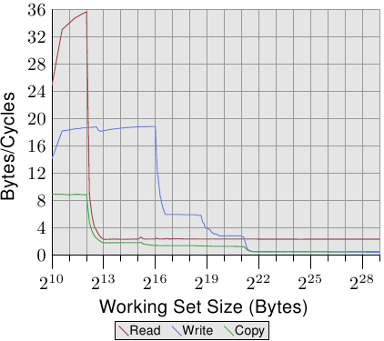
Figure 3.28: AMD Family 10h Opteron Bandwidth
The first detail one notices about the numbers is that the processor
is capable of handling two instructions per cycle if the L1d cache is
sufficient. The read performance exceeds 32 bytes per cycle and even the
write performance is, with 18.7 bytes per cycle, high. The read curve
flattens quickly, though, and is, with 2.3 bytes per cycle, pretty
low. The processor for this test does not prefetch any data, at least
not efficiently.
The write curve on the other hand performs according to the sizes of
the various caches. The peak performance is achieved for the full size
of the L1d, going down to 6 bytes per cycle for L2, to 2.8 bytes per
cycle for L3, and finally .5 bytes per cycle if not even L3 can hold
all the data. The performance for the L1d cache exceeds that of the
(older) Core 2 processor, the L2 access is equally fast (with the
Core 2 having a larger cache), and the L3 and main memory access is
slower.
The copy performance cannot be better than either the read or write
performance. This is why we see the curve initially dominated by the
read performance and later by the write performance.
The multi-thread performance of the Opteron processor is shown in
Figure 3.29.
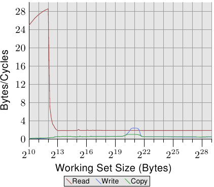
Figure 3.29: AMD Fam 10h Bandwidth with 2 Threads
The read performance is largely
unaffected. Each thread's L1d and L2 works as before and the L3 cache
is in this case not prefetched very well either. The two threads do not
unduly stress the L3 for their purpose. The big problem in this test
is the write performance. All data the threads share has to go
through the L3 cache. This sharing seems to be quite inefficient
since even if the L3 cache size is sufficient to hold the entire
working set the cost is significantly higher than an L3 access.
Comparing this graph with Figure 3.27 we see that the
two threads of the Core 2 processor operate at the speed of the shared
L2 cache for the appropriate range of working set sizes. This level
of performance is achieved for the Opteron processor only for a very
small range of the working set sizes and even here it approaches
only the speed of the L3 which is slower than the Core 2's L2.
3.5.2 Critical Word Load
Memory is transferred from the main memory into the caches in blocks
which are smaller than the cache line size. Today 64 bits are
transferred at once and the cache line size is 64 or 128 bytes. This
means 8 or 16 transfers per cache line are needed.
The DRAM chips can transfer those 64-bit blocks in burst mode. This
can fill the cache line without any further commands from the memory
controller and the possibly associated delays. If the processor
prefetches cache lines this is probably the best way to operate.
If a program's cache access of the data or instruction caches misses
(that means, it is a compulsory cache miss, because the data is used
for the first time, or a capacity cache miss, because the limited
cache size requires eviction of the cache line) the situation is
different. The word inside the cache line which is required for the
program to continue might not be the first word in the cache line.
Even in burst mode and with double data rate transfer the individual
64-bit blocks arrive at noticeably different times. Each block
arrives 4 CPU cycles or more later than the previous one. If the
word the program needs to continue is the eighth of the cache line
the program has to wait an additional 30 cycles or more after the
first word arrives.
Things do not necessarily have to be like this. The memory controller
is free to request the words of the cache line in a different order.
The processor can communicate which word the program is waiting on, the
critical word, and the memory controller can request this word
first. Once the word arrives the program can continue while the rest
of the cache line arrives and the cache is not yet in a consistent
state. This technique is called Critical Word First & Early Restart.
Processors nowadays implement this technique but there are situations when that
is not possible. If the processor prefetches data the critical word
is not known. Should the processor request the cache line during the
time the prefetch operation is in flight it will have to wait until
the critical word arrives without being able to influence the order.
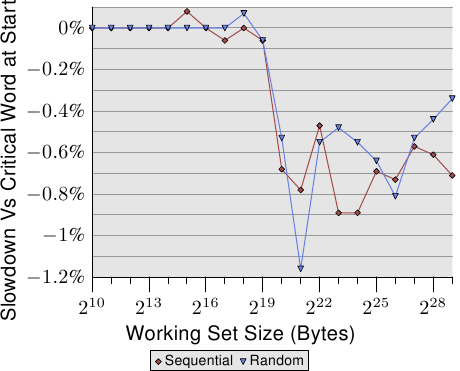
Figure 3.30: Critical Word at End of Cache Line
Even with these optimizations in place the position of the critical
word on a cache line matters. Figure 3.30 shows the
Follow test for sequential and random access. Shown is the slowdown
of running the test with the pointer which is chased in the first
word versus the case when the pointer is in the last word. The
element size is 64 bytes, corresponding the cache line size. The
numbers are quite noisy but it can be seen that, as soon as the L2 is
not sufficient to hold the working set size, the performance of the
case where the critical word is at the end is about 0.7% slower.
The sequential access appears to be affected a bit more. This would be
consistent with the aforementioned problem when prefetching the next
cache line.
3.5.3 Cache Placement
Where the caches are placed in relationship to the hyper-threads,
cores, and processors is not under control of the programmer. But
programmers can determine where the threads are executed and then it
becomes important how the caches relate to the used CPUs.
Here we will not go into details of when to select what cores to run
the threads. We will only describe architecture details which the
programmer has to take into account when setting the affinity of the
threads.
Hyper-threads, by definition share everything but the register set.
This includes the L1 caches. There is not much more to say here. The
fun starts with the individual cores of a processor. Each core has at
least its own L1 caches. Aside from this there are today not many
details in common:
- Early multi-core processors had separate L2 caches and no higher
caches.
- Later Intel models had shared L2 caches for dual-core
processors. For quad-core processors we have to deal with separate L2
caches for each pair of two cores. There are no higher level caches.
- AMD's family 10h processors have separate L2 caches and a unified
L3 cache.
A lot has been written in the propaganda material of the processor
vendors about the advantage of their respective models. Separate L2
caches have an advantage if the working sets handled by the cores do
not overlap. This works well for single-threaded programs. Since
this is still often the reality today this approach does not perform too badly.
But there is always some overlap. The caches all contain the most
actively used parts of the common runtime libraries which means some
cache space is wasted.
Completely sharing all caches beside L1 as Intel's dual-core
processors do can have a big advantage. If the working set of the
threads working on the two cores overlaps significantly the total
available cache memory is increased and working sets can be bigger
without performance degradation. If the working sets do not overlap
Intel's Advanced Smart Cache management is supposed to prevent any one core
from monopolizing the entire cache.
If both cores use about half the cache for their respective working
sets there is some friction, though. The cache constantly has to
weigh the two cores' cache use and the evictions performed as part of
this rebalancing might be chosen poorly. To see the problems we look
at the results of yet another test program.
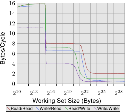
Figure 3.31: Bandwidth with two Processes
The test program has one process constantly reading or writing, using
SSE instructions, a 2MB block of memory. 2MB was chosen because this
is half the size of the L2 cache of this Core 2 processor. The
process is pinned to one core while a second process is pinned to the
other core. This second process reads and writes a memory region of
variable size. The graph shows the number of bytes per cycle which
are read or written. Four different graphs are shown, one for each
combination of the processes reading and writing. The read/write
graph is for the background process, which always uses a 2MB working set
to write, and the measured process with variable working set to read.
The interesting part of the graph is the part between 220 and
223 bytes. If the L2 cache of the two cores were completely
separate we could expect that the performance of all four tests would drop
between 221 and 222 bytes, that means, once the L2 cache is
exhausted. As we can see in Figure 3.31 this is not the
case. For the cases where the background process is writing this is
most visible. The performance starts to deteriorate before the
working set size reaches 1MB. The two processes do not share memory
and therefore the processes do not cause RFO messages to be generated.
These are pure cache eviction problems. The smart cache handling
has its problems with the effect that the experienced cache size per
core is closer to 1MB than the 2MB per core which are available. One
can only hope that, if caches shared between cores remain a feature of
upcoming processors, the algorithm used for the smart cache handling
will be fixed.
Having a quad-core processor with two L2 caches was just a stop-gap
solution before higher-level caches could be introduced. This design
provides no significant performance advantage over separate sockets
and dual-core processors. The two cores communicate via the same bus
which is, at the outside, visible as the FSB. There is no special
fast-track data exchange.
The future of cache design for multi-core processors will lie in more
layers. AMD's 10h family of processors make the start. Whether we will
continue to see lower level caches be shared by a subset of the cores
of a processor remains to be seen. The extra levels of cache are
necessary since the high-speed and frequently used caches cannot be
shared among many cores. The performance would be impacted. It would
also require very large caches with high associativity. Both
numbers, the cache size and the associativity, must scale with the
number of cores sharing the cache. Using a large L3 cache and
reasonably-sized L2 caches is a reasonable trade-off. The L3 cache is
slower but it is ideally not as frequently used as the L2 cache.
For programmers all these different designs mean complexity when
making scheduling decisions. One has to know the workloads and the
details of the machine architecture to achieve the best performance.
Fortunately we have support to determine the machine architecture.
The interfaces will be introduced in later sections.
3.5.4 FSB Influence
The FSB plays a central role in the performance of the machine.
Cache content can only be stored and loaded as quickly as the
connection to the memory allows. We can
show how much so by running a program on two machines which only
differ in the speed of their memory modules. Figure 3.32 shows
the results of the Addnext0 test (adding the content of the next
elements pad[0] element to the own pad[0] element) for
NPAD=7 on a 64-bit machine. Both machines have Intel Core 2
processors, the first uses 667MHz DDR2 modules, the second 800MHz
modules (a 20% increase).
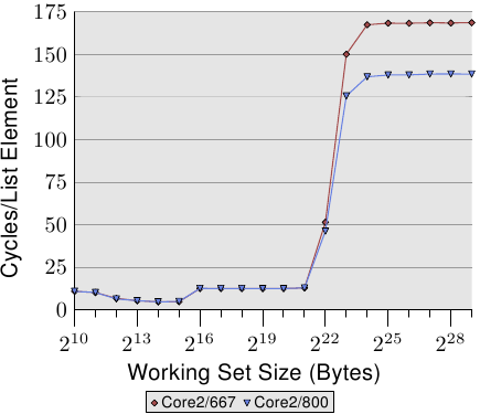
Figure 3.32: Influence of FSB Speed
The numbers show that, when the FSB is really stressed for large
working set sizes, we indeed see a large benefit. The maximum
performance increase measured in this test is 18.2%, close to the
theoretical maximum. What this shows is that a faster FSB indeed can
pay off big time. It is not critical when the working set fits into
the caches (and these processors have a 4MB L2). It must be kept in
mind that we are measuring one program here. The working set of a
system comprises the memory needed by all concurrently running
processes. This way it is easily possible to exceed 4MB memory or
more with much smaller programs.
Today some of Intel's processors support FSB speeds up to
1,333MHz which would mean another 60% increase. The future is going
to see even higher speeds. If speed is important and the working set
sizes are larger, fast RAM and high FSB speeds are certainly worth the
money. One has to be careful, though, since even though the processor
might support higher FSB speeds the motherboard/Northbridge might not.
It is critical to check the specifications.
| 
 LINUX
LINUX